SN74LVTH543DW 供应商
-
SN74LVTH543DW
品牌:TI 封装/批号:原厂原装/22+ -
SN74LVTH543DWR
品牌: 封装/批号:/23+
SN74LVTH543DW 属性参数
- 标准包装:25
- 类别:集成电路 (IC)
- 家庭:逻辑 - 缓冲器,驱动器,接收器,收发器
- 系列:74LVTH
- 逻辑类型:寄存收发器,非反相
- 元件数:1
- 每个元件的位元数:8
- 输出电流高,低:32mA,64mA
- 电源电压:2.7 V ~ 3.6 V
- 工作温度:-40°C ~ 85°C
- 安装类型:表面贴装
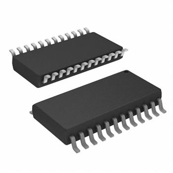
- 封装/外壳:24-SOIC(0.295",7.50mm 宽)
- 供应商设备封装:24-SOIC
- 包装:管件
- 其它名称:296-1717296-1717-5
产品特性
- Support Mixed-Mode Signal Operation (5-V Input and Output Voltages With 3.3-V VCC)
- Typical VOLP (Output Ground Bounce) <0.8 V at VCC = 3.3 V, TA = 25°C
- Support Unregulated Battery Operation Down to 2.7 V
- Ioff and Power-Up 3-State Support Hot Insertion
- Bus Hold on Data Inputs Eliminates the Need for External Pullup/Pulldown Resistors
- Latch-Up Performance Exceeds 500 mA Per JESD 17
- ESD Protection Exceeds JESD 22 2000-V Human-Body Model (A114-A) 200-V Machine Model (A115-A)
- 2000-V Human-Body Model (A114-A)
- 200-V Machine Model (A115-A)
产品概述
These octal transceivers are designed specifically for low-voltage (3.3-V) VCC operation, but with the capability to provide a TTL interface to a 5-V system environment.The ’LVTH543 devices contain two sets of D-type latches for temporary storage of data flowing in either direction. Separate latch-enable (LEAB\ or LEBA\) and output-enable (OEAB\ or OEBA\) inputs are provided for each register, to permit independent control in either direction of data flow.The A-to-B enable (CEAB)\ input must be low to enter data from A or to output data from B. If CEAB\ is low and LEAB\ is low, the A-to-B latches are transparent; a subsequent low-to-high transition of LEAB\ puts the A latches in the storage mode. With CEAB\ and OEAB\ both low, the 3-state B outputs are active and reflect the data present at the output of the A latches. Data flow from B to A is similar, but requires using the CEBA\, LEBA\, and OEBA\ inputs.Active bus-hold circuitry holds unused or undriven inputs at a valid logic state. Use of pullup or pulldown resistors with the bus-hold circuitry is not recommended.When VCC is between 0 and 1.5 V, the device is in the high-impedance state during power up or power down. However, to ensure the high-impedance state above 1.5 V, OE\ should be tied to VCC through a pullup resistor; the minimum value of the resistor is determined by the current-sinking capability of the driver.This device is fully specified for hot-insertion applications using Ioff and power-up 3-state. The Ioff circuitry disables the outputs, preventing damaging current backflow through the device when it is powered down. The power-up 3-state circuitry places the outputs in the high-impedance state during power up and power down, which prevents driver conflict.