SN74LVTH162541DL 供应商
-
SN74LVTH162541DL
品牌:TI 封装/批号:原厂原装/22+
SN74LVTH162541DL 属性参数
- 标准包装:25
- 类别:集成电路 (IC)
- 家庭:逻辑 - 缓冲器,驱动器,接收器,收发器
- 系列:74LVTH
- 逻辑类型:缓冲器/线路驱动器,非反相
- 元件数:2
- 每个元件的位元数:8
- 输出电流高,低:12mA,12mA
- 电源电压:2.7 V ~ 3.6 V
- 工作温度:-40°C ~ 85°C
- 安装类型:表面贴装
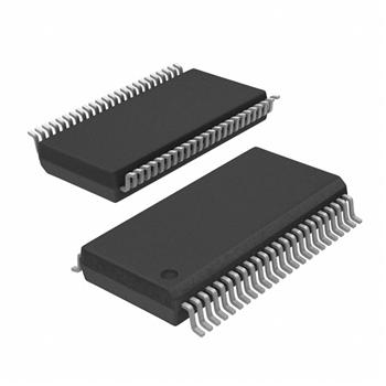
- 封装/外壳:48-BSSOP(0.295",7.50mm 宽)
- 供应商设备封装:48-SSOP
- 包装:管件
- 其它名称:296-8683-5
产品特性
- Members of the Texas Instruments Widebus™ Family
- State-of-the-Art Advanced BiCMOS Technology (ABT) Design for 3.3-V Operation and Low Static-Power Dissipation
- Output Ports Have Equivalent 22- Series Resistors, So No External Resistors Are Required
- Support Mixed-Mode Signal Operation (5-V Input and Output Voltages With 3.3-V VCC)
- Support Unregulated Battery Operation Down to 2.7 V
- Typical VOLP (Output Ground Bounce) <0.8 V at VCC = 3.3 V, TA = 25°C
- Ioff and Power-Up 3-State Support Hot Insertion
- Bus Hold on Data Inputs Eliminates the Need for External Pullup/Pulldown Resistors
- Distributed VCC and GND Pin Configuration Minimizes High-Speed Switching Noise
- Flow-Through Architecture Optimizes PCB Layout
- Latch-Up Performance Exceeds 500 mA Per JESD 17
- ESD Protection Exceeds 2000 V Per MIL-STD-883, Method 3015; Exceeds 200 V Using Machine Model (C = 200 pF, R = 0)
- Package Options Include Plastic Shrink Small-Outline (DL) and Thin Shrink Small-Outline (DGG) Packages and 380-mil Fine-Pitch Ceramic Flat (WD) Package Using 25-mil Center-to-Center Spacings
产品概述
These 16-bit buffers/drivers are designed specifically for low-voltage (3.3-V) VCC operation, but with the capability to provide a TTL interface to a 5-V system environment.These devices are noninverting 16-bit buffers composed of two 8-bit sections with separate output-enable signals. For either 8-bit buffer section, the two output-enable (1OE1 and 1OE2 or 2OE1 and 2OE2) inputs must be low for the corresponding Y outputs to be active. If either output-enable input is high, the outputs of that 8-bit buffer section are in the high-impedance state.The outputs, which are designed to source or sink up to 12 mA, include equivalent 22- series resistors to reduce overshoot and undershoot.When VCC is between 0 and 1.5 V, the devices are in the high-impedance state during power up or power down. However, to ensure the high-impedance state above 1.5 V, OE should be tied to VCC through a pullup resistor; the minimum value of the resistor is determined by the current-sinking capability of the driver.Active bus-hold circuitry is provided to hold unused or floating data inputs at a valid logic level.These devices are fully specified for hot-insertion applications using Ioff and power-up 3-state. The Ioff circuitry disables the outputs, preventing damaging current backflow through the devices when they are powered down. The power-up 3-state circuitry places the outputs in the high-impedance state during power up and power down, which prevents driver conflict.The SN54LVTH162541 is characterized for operation over the full military temperature range of -55°C to 125°C. The SN74LVTH162541 is characterized for operation from -40°C to 85°C.