SN74LVT543DW 供应商
-
SN74LVT543DW
品牌:TI 封装/批号:原厂原装/22+
SN74LVT543DW 属性参数
- 标准包装:25
- 类别:集成电路 (IC)
- 家庭:逻辑 - 缓冲器,驱动器,接收器,收发器
- 系列:74LVT
- 逻辑类型:寄存收发器,非反相
- 元件数:1
- 每个元件的位元数:8
- 输出电流高,低:32mA,64mA
- 电源电压:2.7 V ~ 3.6 V
- 工作温度:-40°C ~ 85°C
- 安装类型:表面贴装
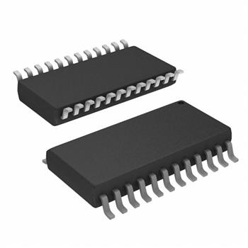
- 封装/外壳:24-SOIC(0.295",7.50mm 宽)
- 供应商设备封装:24-SOIC
- 包装:管件
产品特性
- State-of-the-Art Advanced BiCMOS Technology (ABT) Design for 3.3-V Operation and Low Static Power Dissipation
- Support Mixed-Mode Signal Operation (5-V Input and Output Voltages With 3.3-V VCC)
- Support Unregulated Battery Operation Down to 2.7 V
- Typical VOLP (Output Ground Bounce)< 0.8 V at VCC = 3.3 V, TA = 25°C
- ESD Protection Exceeds 2000 V Per MIL-STD-883C, Method 3015; Exceeds 200 V Using Machine Model (C = 200 pF, R = 0)
- Latch-Up Performance Exceeds 500 mA Per JEDEC Standard JESD-17
- Bus-Hold Data Inputs Eliminate the Need for External Pullup Resistors
- Support Live Insertion
- Package Options Include Plastic Small-Outline (DW), Shrink Small-Outline (DB), and Thin Shrink Small-Outline (PW) Packages, Ceramic Chip Carriers (FK), and Ceramic (JT) DIPs
产品概述
These octal transceivers are designed specifically for low-voltage
(3.3-V) VCC operation, but with the capability to provide
a TTL interface to a 5-V system environment.The 'LVT543 contain two sets of D-type latches for temporary
storage of data flowing in either direction. Separate latch-enable
(or) and output-enable(or) inputs are
provided for each register to permit independent control in either
direction of data flow.The A-to-B enable ()
input must be low in order to enter data from A or to output data
from B. If is low and
is low, the
A-to-B latches are transparent; a subsequent low-to-high transition
of puts the A
latches in the storage mode. With and both low, the
3-state B outputs are active and reflect the data present at the
output of the A latches. Data flow from B to A is similar but
requires using the ,, and inputs.Active bus-hold circuitry is provided to hold unused or floating
data inputs at a valid logic level.To ensure the high-impedance state during power up or power down,
should be tied
to VCC through a pullup resistor; the minimum value of the
resistor is determined by the current-sinking capability of the
driver.The SN74LVT543 is available in TI's shrink small-outline package
(DB), which provides the same I/O pin count and functionality of
standard small-outline packages in less than half the
printed-circuit-board area.The SN54LVT543 is characterized for operation over the full
military temperature range of -55°C to 125°C. The
SN74LVT543 is characterized for operation from -40°C to
85°C.