SN74LS07DBR 供应商
-
SN74LS07DBR
品牌:TI 封装/批号:原厂原装/22+ -
SN74LS07DBR
品牌:TI 封装/批号:SSOP/23+ -
SN74LS07DBR
品牌: 封装/批号:TSSOP/23+ -
SN74LS07DBR
品牌:TI 封装/批号:14-SSOP/21+ -
SN74LS07DBR
品牌: 封装/批号:SSOP14/2019+ -
SN74LS07DBR
品牌:TI(德州仪器) 封装/批号:SSOP-14_208mil/2022+ -
SN74LS07DBR
品牌:TI代理 封装/批号:SSOP14/23+ -
SN74LS07DBRG4
品牌:TI 封装/批号:/22+
SN74LS07DBR 属性参数
- 标准包装:1
- 类别:集成电路 (IC)
- 家庭:逻辑 - 缓冲器,驱动器,接收器,收发器
- 系列:74LS
- 逻辑类型:缓冲器/线路驱动器,非反相
- 元件数:6
- 每个元件的位元数:1
- 输出电流高,低:40mA,40mA
- 电源电压:4.75 V ~ 5.25 V
- 工作温度:0°C ~ 70°C
- 安装类型:表面贴装
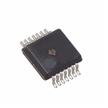
- 封装/外壳:14-SSOP(0.209",5.30mm 宽)
- 供应商设备封装:14-SSOP
- 包装:®
- 其它名称:296-3627-6
产品特性
- Convert TTL Voltage Levels to MOS Levels
- High Sink-Current Capability
- Input Clamping Diodes Simplify System Design
- Open-Collector Driver for Indicator Lamps and Relays
产品概述
These hex buffers and drivers feature high-voltage open-collector outputs to interface
with high-level circuits or for driving high-current loads. They are also characterized for use as
buffers for driving TTL inputs. The SN74LS07 devices have a rated output voltage of 30 V. The
maximum sink current is 40 mA.These circuits are compatible with most TTL families. Inputs are diode-clamped to
minimize transmission-line effects, which simplifies design. Typical power dissipation is 140 mW,
and average propagation delay time is 12 ns.
SN74LS07DBR 数据手册
SN74LS07DBR 电路图