SN74BCT25244DWR 供应商
-
SN74BCT25244DWR
品牌:TI 封装/批号:原厂原装/22+ -
SN74BCT25244DWR
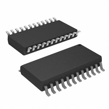
品牌:TI(德州仪器) 封装/批号:SOIC-24/2022+
SN74BCT25244DWR 属性参数
- 标准包装:2,000
- 类别:集成电路 (IC)
- 家庭:逻辑 - 缓冲器,驱动器,接收器,收发器
- 系列:74BCT
- 逻辑类型:缓冲器/线路驱动器,非反相
- 元件数:2
- 每个元件的位元数:4
- 输出电流高,低:80mA,188mA
- 电源电压:4.5 V ~ 5.5 V
- 工作温度:0°C ~ 70°C
- 安装类型:表面贴装
- 封装/外壳:24-SOIC(0.295",7.50mm 宽)
- 供应商设备封装:24-SOIC
- 包装:带卷 (TR)
产品特性
- State-of-the-Art BiCMOS Design Significantly Reduces ICCZ
- ESD Protection Exceeds 2000 V Per MIL-STD-883C, Method 3015; Exceeds 200 V Using Machine Model (C = 200 pF, R = 0)
- Designed to Facilitate Incident-Wave Switching for Line Impedances of 25 or Greater
- Distributed VCC and GND Pins Minimize Noise Generated by the Simultaneous Switching of Outputs
- Package Options Include Plastic Small-Outline (DW) Packages, Ceramic Chip Carriers (FK) and Flatpacks (W), and Standard Plastic and Ceramic 300-mil DIPs (JT, NT)
产品概述
These 25- octal buffers
and line drivers are designed specifically to improve both the
performance and density of 3-state memory address drivers, clock
drivers, and bus-oriented receivers and transmitters.These buffers are capable of sinking 188-mA IOL, which
facilitates switching 25-
transmission lines on the incident wave. The distributed
VCC and GND pins minimize switching noise for more
reliable system operation.When the output-enable (1 and
2) inputs are
low, the device transmits data from the A inputs to the Y outputs.
When 1 and 2 are high, the outputs are in the
high-impedance state.The SN54BCT25244 is characterized for operation over the full
military temperature range of -55°C to 125°C. The
SN74BCT25244 is characterized for operation from 0°C to
70°C.