SN74AUC126RGYR 供应商
-
SN74AUC126RGYR
品牌:TI 封装/批号:原厂原装/22+
SN74AUC126RGYR 属性参数
- 标准包装:1
- 类别:集成电路 (IC)
- 家庭:逻辑 - 缓冲器,驱动器,接收器,收发器
- 系列:74AUC
- 逻辑类型:缓冲器/线路驱动器,非反相
- 元件数:4
- 每个元件的位元数:1
- 输出电流高,低:9mA,9mA
- 电源电压:0.8 V ~ 2.7 V
- 工作温度:-40°C ~ 85°C
- 安装类型:表面贴装
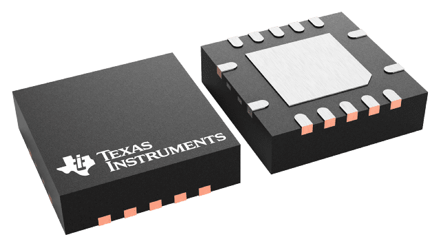
- 封装/外壳:14-VFQFN 裸露焊盘
- 供应商设备封装:14-VQFN 裸露焊盘(3.5x3.5)
- 包装:®
- 其它名称:296-18543-6
产品特性
- Optimized for 1.8-V Operation and Is 3.6-V I/O Tolerant to Support Mixed-Mode Signal Operation
- Ioff Supports Partial-Power-Down Mode Operation
- Sub 1-V Operable
- Max tpd of 2.1 ns at 1.8 V
- Low Power Consumption, 10-µA Max ICC
- ±8-mA Output Drive at 1.8 V
- Latch-Up Performance Exceeds 100 mA Per JESD 78, Class II
- ESD Protection Exceeds JESD 22 2000-V Human-Body Model (A114-A) 200-V Machine Model (A115-A) 1500-V Charged-Device Model (C101)
- 2000-V Human-Body Model (A114-A)
- 200-V Machine Model (A115-A)
- 1500-V Charged-Device Model (C101)
产品概述
This quadruple bus buffer gate is designed for 0.8-V to 2.7-V VCC operation, but is designed specifically for 1.6-V to 1.95-V VCC operation.The SN74AUC126 contains four independent line drivers with 3-state outputs. Each output is disabled when the associated output-enable (OE) input is low.To ensure the high-impedance state during power up or power down, OE should be tied to GND through a pulldown resistor; the minimum value of the resistor is determined by the current-sourcing capability of the driver.This device is fully specified for partial-power-down applications using Ioff. The Ioff circuitry disables the outputs, preventing damaging current backflow through the device when it is powered down.