SN74AS286D 供应商
-
SN74AS286D
品牌:TI 封装/批号:原厂原装/22+
SN74AS286D 属性参数
- 标准包装:50
- 类别:集成电路 (IC)
- 家庭:逻辑 - 奇偶校验发生器和校验器
- 系列:74AS
- 逻辑类型:奇偶校验发生器/校验器
- 电路数:9 位
- 输出电流高,低:15mA,48mA; 2mA,20mA
- 电源电压:4.5 V ~ 5.5 V
- 工作温度:0°C ~ 70°C
- 安装类型:表面贴装
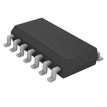
- 封装/外壳:14-SOIC(0.154",3.90mm 宽)
- 供应商设备封装:14-SOIC
产品特性
- Generate Either Odd or Even Parity forNine Data Lines
- Cascadable for n-Bit Parity
- Direct Bus Connection for Parity Generation or Checking by Using the Parity I/O Port
- Glitch-Free Bus During Power Up/Down
- Package Options Include Plastic Small-Outline (D) Packages, Ceramic Chip Carriers (FK), and Standard Plastic (N) and Ceramic (J) 300-mil DIPs
产品概述
The SN54AS286 and SN74AS286 universal 9-bit parity
generators/checkers feature a local output for parity checking and a
48-mA bus-driving
parity input/output (I/O) port for parity generation/checking. The
word-length capability is easily expanded by cascading.The transmit () control input
is implemented specifically to accommodate cascading. When is low, the parity tree is
disabled and PARITY ERROR remains at a high logic level regardless of
the input levels. When is
high, the parity tree is enabled. PARITY ERROR indicates a parity
error when either an even number of inputs (A-I) are high and PARITY
I/O is forced to a low logic level, or when an odd number of inputs
are high and PARITY I/O is forced to a high logic level.The I/O control circuitry was designed so that the I/O port
remains in the high-impedance state during power up or power down to
prevent bus glitches.The SN54AS286 is characterized for operation over the full
military temperature range of -55°C to 125°C. The SN74AS286
is characterized for operation from 0°C to 70°C.