SN74ABT16827DLR 供应商
-
SN74ABT16827DLR
品牌:TI 封装/批号:原厂原装/22+ -
SN74ABT16827DLR
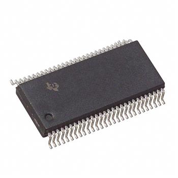
品牌:TI(德州仪器) 封装/批号:SSOP-56/2022+
SN74ABT16827DLR 属性参数
- 标准包装:1
- 类别:集成电路 (IC)
- 家庭:逻辑 - 缓冲器,驱动器,接收器,收发器
- 系列:74ABT
- 逻辑类型:缓冲器/线路驱动器,非反相
- 元件数:2
- 每个元件的位元数:10
- 输出电流高,低:32mA,64mA
- 电源电压:4.5 V ~ 5.5 V
- 工作温度:-40°C ~ 85°C
- 安装类型:表面贴装
- 封装/外壳:56-BSSOP(0.295",7.50mm 宽)
- 供应商设备封装:56-SSOP
- 包装:®
- 其它名称:296-3928-6
产品特性
- Members of the Texas Instruments WidebusTM Family
- State-of-the-Art EPIC-II BTM BiCMOS Design Significantly Reduces Power Dissipation
- Latch-Up Performance Exceeds 500 mA Per JEDEC Standard JESD-17
- Typical VOLP (Output Ground Bounce) < 1 V at VCC = 5 V, TA = 25°C
- High-Impedance State During Power Up and Power Down
- Distributed VCC and GND Pin Configuration Minimizes High-Speed Switching Noise
- Flow-Through Architecture Optimizes PCB Layout
- High-Drive Outputs (-32-mA IOH, 64-mA IOL)
- Package Options Include Plastic 300-mil Shrink Small-Outline (DL) Package and 380-mil Fine-Pitch Ceramic Flat (WD) Package Using 25-mil Center-to-Center Spacings Widebus and EPIC-IIB are trademarks of Texas Instruments Incorporated.
产品概述
The 'ABT16827 are noninverting 20-bit buffers composed of two 10-bit sections with separate output-enable signals. For either 10-bit buffer section, the two output-enable (1OE1\ and 1OE2\ or 2OE1\ and 2OE2\) inputs must both be low for the corresponding Y outputs to be active. If either output-enable input is high, the outputs of that 10-bit buffer section are in the high-impedance state.
When VCC is between 0 and 2.1 V, the device is in the high-impedance state during power up or power down. However, to ensure the high-impedance state above 2.1 V, OE\ should be tied to VCC through a pullup resistor; the minimum value of the resistor is determined by the current-sinking capability of the driver.
The SN54ABT16827 is characterized for operation over the full military temperature range of -55°C to 125°C. The SN74ABT16827 is characterized for operation from -40°C to 85°C.