CLVTH16245AQDLREP 供应商
-
CLVTH16245AQDLREP
品牌:TI 封装/批号:原厂原装/22+ -
CLVTH16245AQDLREP
品牌:TI 封装/批号:SSOP/新批号
CLVTH16245AQDLREP 属性参数
- 标准包装:1
- 类别:集成电路 (IC)
- 家庭:逻辑 - 缓冲器,驱动器,接收器,收发器
- 系列:74LVTH
- 逻辑类型:收发器,非反相
- 元件数:2
- 每个元件的位元数:8
- 输出电流高,低:24mA,24mA
- 电源电压:2.7 V ~ 3.6 V
- 工作温度:-40°C ~ 125°C
- 安装类型:表面贴装
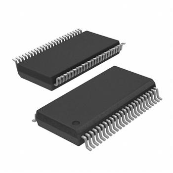
- 封装/外壳:48-BSSOP(0.295",7.50mm 宽)
- 供应商设备封装:48-SSOP
- 包装:®
- 其它名称:296-22131-6
产品特性
- Controlled BaselineOne AssemblyOne Test SiteOne Fabrication Site
- One Assembly
- One Test Site
- One Fabrication Site
- Enhanced Diminishing Manufacturing Sources (DMS) Support
- Enhanced Product-Change Notification
- Qualification Pedigree(1)
- Member of the Texas Instruments Widebus™ Family
- State-of-the-Art Advanced BiCMOS Technology (ABT) Design for 3.3-V Operation and Low Static-Power Dissipation
- Supports Mixed-Mode Signal Operation (5-V Input and Output Voltages With 3.3-V VCC)
- Supports Unregulated Battery Operation Down to 2.7 V
- Typical VOLP (Output Ground Bounce) <0.8 V at VCC = 3.3 V, TA = 25°C
- Distributed VCC and GND Pins Minimize High-Speed Switching Noise
- Flow-Through Architecture Optimizes PCB Layout
- Ioff and Power-Up 3-State Support Hot Insertion
- Bus Hold on Data Inputs Eliminates the Need for External Pullup/Pulldown Resistors
- Latch-Up Performance Exceeds 500 mA Per JESD 17
- ESD Protection Exceeds JESD 222000-V Human-Body Model (A114-A)200-V Machine Model (A115-A)
- 2000-V Human-Body Model (A114-A)
- 200-V Machine Model (A115-A)
产品概述
The SN74LVTH16245A is a 16-bit (dual-octal) noninverting 3-state transceiver designed for low-voltage (3.3-V) VCC operation, but with the capability to provide a TTL interface to a 5-V system environment.This device can be used as two 8-bit transceivers or one 16-bit transceiver. It allows data transmission from the A bus to the B bus or from the B bus to the A bus, depending on the logic level at the direction-control (DIR) input. The output-enable (OE) input can be used to disable the devices so that the buses effectively are isolated.Active bus-hold circuitry holds unused or undriven inputs at a valid logic state. Use of pullup or pulldown resistors with the bus-hold circuitry is not recommended.When VCC is between 0 V and 1.5 V, the device is in the high-impedance state during power up or power down. However, to ensure the high-impedance state above 1.5 V, OE should be tied to VCC through a pullup resistor; the minimum value of the resistor is determined by the current-sinking capability of the driver.This device is fully specified for hot-insertion applications using Ioff and power-up 3-state. The Ioff circuitry disables the outputs, preventing damaging current backflow through the device when it is powered down. The power-up 3-state circuitry places the outputs in the high-impedance state during power up and power down, which prevents driver conflict.