CLVC2G125IDCURQ1 供应商
-
CLVC2G125IDCURQ1
品牌:TI 封装/批号:原厂原装/22+ -
CLVC2G125IDCURQ1
品牌:TI(德州仪器) 封装/批号:VSSOP-8/2022+
CLVC2G125IDCURQ1 属性参数
- 标准包装:1
- 类别:集成电路 (IC)
- 家庭:逻辑 - 缓冲器,驱动器,接收器,收发器
- 系列:74LVC
- 逻辑类型:缓冲器/线路驱动器,非反相
- 元件数:2
- 每个元件的位元数:1
- 输出电流高,低:32mA,32mA
- 电源电压:1.65 V ~ 5.5 V
- 工作温度:-40°C ~ 85°C
- 安装类型:表面贴装
- 封装/外壳:8-VFSOP(0.091",2.30mm 宽)
- 供应商设备封装:US8
- 包装:®
- 其它名称:296-28411-6
产品特性
- Qualified for Automotive Applications
- Supports 5-V VCC Operation
- Inputs Accept Voltages to 5.5 V
- Max tpd of 4.3 ns at 3.3 V
- Low Power Consumption, 10-µA Max ICC
- ±24-mA Output Drive at 3.3 V
- Typical VOLP (Output Ground Bounce) <0.8 V at VCC = 3.3 V, TA = 25°C
- Typical VOHV (Output VOH Undershoot) >2 V at VCC = 3.3 V, TA = 25°C
- Ioff Supports Partial-Power-Down Mode Operation
- Latch-Up Performance Exceeds 100 mA Per JESD 78, Class II
产品概述
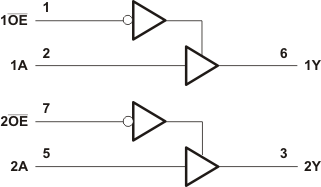
The SN74LVC2G125-Q1 is a dual bus buffer gate designed for 1.65-V to 5.5-V VCC operation. This device features dual line drivers with 3-state outputs. The outputs are disabled when the associated output-enable (OE) input is high.To ensure the high-impedance state during power up or power down, OE should be tied to VCC through a pullup resistor; the minimum value of the resistor is determined by the current-sinking capability of the driver.This device is fully specified for partial-power-down applications using Ioff. The Ioff circuitry disables the outputs, preventing damaging current backflow through the device when it is powered down.
CLVC2G125IDCURQ1 电路图