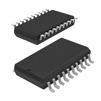
CD74FCT541M 供应商
-
CD74FCT541M
品牌:TI 封装/批号:原厂原装/22+
CD74FCT541M 属性参数
- 标准包装:25
- 类别:集成电路 (IC)
- 家庭:逻辑 - 缓冲器,驱动器,接收器,收发器
- 系列:74FCT
- 逻辑类型:缓冲器/线路驱动器,非反相
- 元件数:1
- 每个元件的位元数:8
- 输出电流高,低:15mA,64mA
- 电源电压:4.75 V ~ 5.25 V
- 工作温度:0°C ~ 70°C
- 安装类型:表面贴装
- 封装/外壳:20-SOIC(0.295",7.50mm 宽)
- 供应商设备封装:20-SOIC
- 包装:管件
- 其它名称:296-33014-5CD74FCT541M-ND
产品特性
- BiCMOS Technology With Low Quiescent Power
- Buffered Inputs
- Noninverted Outputs
- Input/Output Isolation From VCC
- Controlled Output Edge Rates
- 64-mA Output Sink Current
- Output Voltage Swing Limited to 3.7 V
- SCR Latch-Up-Resistant BiCMOS Process and Circuit Design
- Package Options Include Plastic Small-Outline (M) and Shrink Small-Outline (SM) Packages and Standard Plastic (E) DIP
产品概述
The CD74FCT541 is an octal buffer/driver with 3-state outputs that is ideal for driving bus lines or buffer memory address registers and uses a small-geometry BiCMOS technology. The output stage is a combination of bipolar and CMOS transistors that limits the output high level to two diode drops below VCC. This resultant lowering of output swing (0 V to 3.7 V) reduces power-bus ringing [a source of electromagnetic interference (EMI)] and minimizes VCC bounce and ground bounce and their effects during simultaneous output switching. The output configuration also enhances switching speed and is capable of sinking 64 mA.
The 3-state control gate is a two-input AND gate with active-low inputs, so that if either output-enable (OE1\ or OE2\) input is high, all corresponding outputs are in the high-impedance state. The outputs provide noninverted data when they are not in the high-impedance state.
To ensure the high-impedance state during power up or power down, OE\ should be tied to VCC through a pullup resistor; the minimum value of the resistor is determined by the current-sinking capability of the driver.
The CD74FCT541 is characterized for operation from 0°C to 70°C.
