74AUP1G125DCKRG4 供应商
-
74AUP1G125DCKRG4
品牌:TI 封装/批号:原厂原装/22+ -
74AUP1G125DCKRG4
品牌:TI(德州仪器) 封装/批号:SC-70-5/2022+
74AUP1G125DCKRG4 属性参数
- 标准包装:3,000
- 类别:集成电路 (IC)
- 家庭:逻辑 - 缓冲器,驱动器,接收器,收发器
- 系列:74AUP
- 逻辑类型:缓冲器/线路驱动器,非反相
- 元件数:1
- 每个元件的位元数:1
- 输出电流高,低:4mA,4mA
- 电源电压:0.8 V ~ 3.6 V
- 工作温度:-40°C ~ 85°C
- 安装类型:表面贴装
- 封装/外壳:6-TSSOP(5 引线),SC-88A,SOT-353
- 供应商设备封装:SC-70-5
- 包装:带卷 (TR)
产品特性
- Available in the Texas Instruments NanoStar™ Package
- Low Static-Power Consumption (ICC = 0.9 µA Maximum)
- Low Dynamic-Power Consumption (Cpd = 4 pF Typical at 3.3 V)
- Low Input Capacitance (CI = 1.5 pF Typical)
- Low Noise – Overshoot and Undershoot < 10% of VCC
- Input-Disable Feature Allows Floating Input Conditions
- Ioff Supports Partial-Power-Down Mode Operation
- Input Hysteresis Allows Slow Input Transition and Better Switching Noise Immunity at Input
- Wide Operating VCC Range of 0.8 V to 3.6 V
- 3.6-V I/O Tolerant to Support Mixed-Mode Signal Operation
- tpd = 4.6 ns Maximum at 3.3 V
产品概述
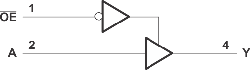
The SN74AUP1G125 bus buffer gate is a single line driver with a 3-state
output. The output is disabled when the output-enable (OE) input is high.
This device has the input-disable feature, which allows floating input signals.To ensure the high-impedance state during power up or power down,
OE must be tied to VCC through a pullup resistor; the
minimum value of the resistor is determined by the current-sinking capability of the driver.
74AUP1G125DCKRG4 电路图