TXS0101DCKT 供应商
-
TXS0101DCKT
品牌:TI 封装/批号:原厂原装/22+ -
TXS0101DCKT
品牌:TI 封装/批号:SC-70-6/ -
TXS0101DCKT
品牌:TI 封装/批号:SC70-6/21+
TXS0101DCKT 属性参数
- 标准包装:1
- 类别:集成电路 (IC)
- 家庭:逻辑 - 变换器
- 系列:-
- 逻辑功能:变换器,双向,开路漏极
- 位数:1
- 输入类型:电压
- 输出类型:电压
- 数据速率:24Mbps
- 通道数:1
- 输出/通道数目:1
- 差分 - 输入:输出:无/无
- 传输延迟(最大):4.6ns
- 电源电压:1.65 V ~ 3.6 V,2.3 V ~ 5.5 V
- 工作温度:-40°C ~ 85°C
- 封装/外壳:*
- 供应商设备封装:*
- 包装:*
- 其它名称:296-32602-6
产品特性
- Latch-Up Performance Exceeds 100 mA Per JESD 78, Class II
- ESD Protection Exceeds JESD 22 A Port 2500 V Human-Body Model (A114-B) 200 V Machine Model (A115-A) 1500 V Charged-Device Model (C101) B Port 8 kV Human-Body Model (A114-B) 200 V Machine Model (A115-A) 1500 V Charged-Device Model (C101)
- A Port 2500 V Human-Body Model (A114-B) 200 V Machine Model (A115-A) 1500 V Charged-Device Model (C101)
- 2500 V Human-Body Model (A114-B)
- 200 V Machine Model (A115-A)
- 1500 V Charged-Device Model (C101)
- B Port 8 kV Human-Body Model (A114-B) 200 V Machine Model (A115-A) 1500 V Charged-Device Model (C101)
- 8 kV Human-Body Model (A114-B)
- 200 V Machine Model (A115-A)
- 1500 V Charged-Device Model (C101)
- No Direction-Control Signal Needed
- Maximum Data Rates 24 Mbps (Push Pull) 2 Mbps (Open Drain)
- 24 Mbps (Push Pull)
- 2 Mbps (Open Drain)
- Available in the Texas Instruments NanoFree™ Package
- 1.65 V to 3.6 V on A port and 2.3 V to 5.5 V on B port (VCCA ≤ VCCB)
- VCC Isolation Feature – If Either VCC Input Is at GND, Both Ports Are in the High-Impedance State
- No Power-Supply Sequencing Required – Either VCCA or VCCB Can be Ramped First
- Ioff Supports Partial-Power-Down Mode Operation
产品概述
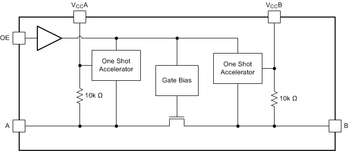
This one-bit non-inverting translator uses two separate configurable power-supply rails.
The A port is designed to track VCCA. VCCA accepts
any supply voltage from 1.65 V to 3.6 V. The B port is designed to track
VCCB. VCCA must be less than or equal to
VCCB. VCCB accepts any supply voltage from 2.3 V to
5.5 V. This allows for low voltage bidirectional translation between any of the 1.8 V, 2.5 V, 3.3
V, and 5 V voltage nodes.When the output-enable (OE) input is low, all outputs are placed in the high-impedance
state.To ensure the high-impedance state during power up or power down, OE should be tied to
GND through a pull-down resistor; the minimum value of the resistor is determined by the
current-sourcing capability of the driver.
TXS0101DCKT 数据手册
TXS0101DCKT 电路图