TPS65123RGTR 供应商
-
TPS65123RGTR
品牌:TI 封装/批号:原厂原装/22+ -
TPS65123RGTR
品牌:TI 封装/批号:QFN-16/7 -
TPS65123RGTR
品牌:TI 封装/批号:/2019+ -
TPS65123RGTR
品牌:TI(德州仪器) 封装/批号:VQFN/2022+ -
TPS65123RGTR
品牌:TI 封装/批号:SMD/23+ -
TPS65123RGTR
品牌:TI 封装/批号:VQFN/21+ -
TPS65123RGTRGE
品牌:TI 封装/批号:/23+
TPS65123RGTR 属性参数
- 标准包装:1
- 类别:集成电路 (IC)
- 家庭:PMIC - 稳压器 - 专用型
- 系列:-
- 应用:转换器,TFT,LCD
- 输入电压:2.5 V ~ 5.5 V
- 输出数:4
- 输出电压:3V ~ 5.6V,最高可调至 20V,最低可调至 -18V
- 工作温度:-40°C ~ 85°C
- 安装类型:表面贴装
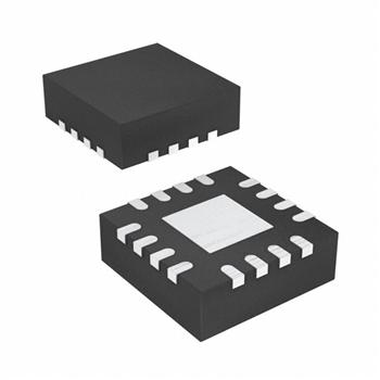
- 封装/外壳:16-VFQFN 裸露焊盘
- 供应商设备封装:16-QFN-EP(3x3)
- 包装:®
- 其它名称:296-17183-6
产品特性
- Main Output, VMAIN Adjustable Voltage, 3.0 V to 5.6 V/25 mA Post-Regulated for Low Ripple (5mVPP) ±0.8% Typical Accuracy Efficiency up to 83%
- Adjustable Voltage, 3.0 V to 5.6 V/25 mA
- Post-Regulated for Low Ripple (5mVPP)
- ±0.8% Typical Accuracy
- Efficiency up to 83%
- Positive Output, VGH Adjustable Voltage up to 20 V/2 mA ±3% Typical Accuracy
- Adjustable Voltage up to 20 V/2 mA
- ±3% Typical Accuracy
- Negative Output, VGL Adjustable Voltage down to -18 V/2 mA ±3% Typical Accuracy
- Adjustable Voltage down to -18 V/2 mA
- ±3% Typical Accuracy
- Auxiliary 1.8 V/3.3 V Linear Regulator
- Automatic or Programmable Power Sequencing
- Complete 1 mm Component Profile Solution
- 2.5 V to 5.5 V Input Voltage Range
- Output Short Circuit Protected
- 16-Pin QFN Package (3 × 3 × 0,9 mm)
- APPLICATIONS Small Form Factor a-Si and LTPS TFT LCD Cell Phones, Smart Phones PDAs, Pocket PCs Portable DVD Digital-Still Cameras, Camcorders Handheld Instruments Portable GPS Car Navigation Systems
- Small Form Factor a-Si and LTPS TFT LCD
- Cell Phones, Smart Phones
- PDAs, Pocket PCs
- Portable DVD
- Digital-Still Cameras, Camcorders
- Handheld Instruments
- Portable GPS
- Car Navigation Systems
产品概述
The TPS6512x DC-DC converter supplies all three voltages required by amorphous-silicon (a-Si) and low-temperature poly-silicon (LTPS) TFT-LCD displays. The compact layout of the TPS6512x uses a single inductor to generate independently-regulated positive and negative outputs. A free-running variable peak current PWM control scheme time-multiplexes the inductor between outputs. This control architecture operates at a pseudo-fixed-frequency to provide fast response to line and load transients while maintaining a relatively constant switching frequency and high efficiency over a wide range of input and output voltages. Due to the high switching frequency capability of the device, inexpensive and ultra-thin 8.2 or 10 µH inductors can be used.The main output, VMAIN, is post-regulated to provide a low-ripple source drive voltage for the LCD display. The auxiliary outputs generate a boosted output voltage, VGH, up to 20 V, and a negative output voltage, VGL, down to -18 V for the LCD gate drive. The device has internal current limiting for high reliability under fault conditions. Additionally, the device offers a fixed output linear regulator for the LCD logic circuitry.