TPS57040QDGQRQ1 供应商
-
TPS57040QDGQRQ1
品牌:TI 封装/批号:MSOP-10/23+ -
TPS57040QDGQRQ1
品牌:TI 封装/批号:MSOP10/24+ -
TPS57040QDGQRQ1
品牌:TI 封装/批号:/22+ -
TPS57040QDGQRQ1
品牌:TI(德州仪器) 封装/批号:MSOP-PowerPad-10/2022+ -
TPS57040QDGQRQ1
品牌:TI 封装/批号:原封/23+ -
TPS57040QDGQRQ1
品牌:TI 封装/批号:MSOP-10/22+ -
TPS57040QDGQRQ1
品牌:TI 封装/批号:HVSSOP-10/23+ -
TPS57040QDGQRQ1/MSOP10
品牌:TI(德州仪器) 封装/批号:/20+
TPS57040QDGQRQ1 属性参数
- 标准包装:1
- 类别:集成电路 (IC)
- 家庭:PMIC - 稳压器 - DC DC 开关稳压器
- 系列:SWIFT™, Eco-Mode™
- 类型:降压(降压)
- 输出类型:可调式
- 输出数:1
- 输出电压:0.8 V ~ 39 V
- 输入电压:3.5 V ~ 42 V
- PWM 型:电流模式
- 频率 - 开关:581kHz
- 电流 - 输出:500mA
- 同步整流器:无
- 工作温度:-40°C ~ 150°C
- 安装类型:表面贴装
- 封装/外壳:10-TFSOP,10-MSOP(0.118",3.00mm 宽)裸露焊盘
- 包装:®
- 供应商设备封装:10-MSOP-PowerPad
- 其它名称:296-28154-6
产品特性
- Qualified for Automotive Applications
- AEC-Q100 Qualified With the Following Results Device Temperature Grade 1: –40°C to 125°C Ambient Operating Temperature Range Device HBM ESD Classification Level 2 Device CDM ESD Classification Level C4B
- Device Temperature Grade 1: –40°C to 125°C Ambient Operating Temperature Range
- Device HBM ESD Classification Level 2
- Device CDM ESD Classification Level C4B
- 3.5-V to 42-V Input Voltage Range
- 200-mΩ High-Side MOSFET
- High Efficiency at Light Loads with a Pulse Skipping Eco-mode™ Control Scheme
- 116-µA Operating Quiescent Current
- 1.5-µA Shutdown Current
- 100-kHz to 2.5-MHz Switching Frequency
- Synchronizes to External Clock
- Adjustable Slow Start/Sequencing
- Undervoltage and Overvoltage Power-good Output
- Adjustable Undervoltage Lockout Voltage and Hysteresis
- 0.8-V Internal Voltage Reference
- Supported by SwitcherPro™ Software Tool (http://focus.ti.com/docs/toolsw/folders/print/switcherpro.html)
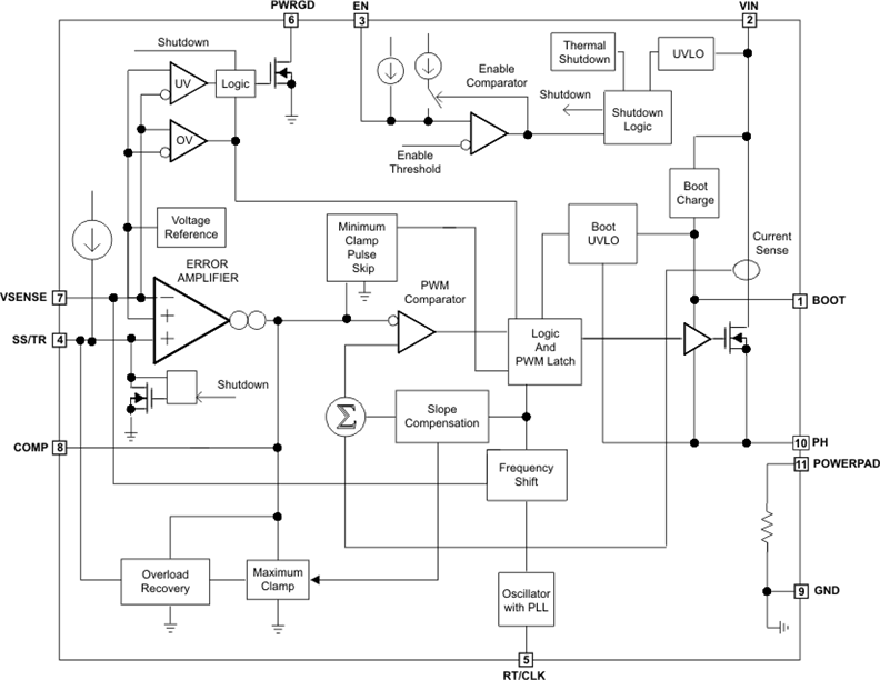
产品概述
The TPS57040-Q1 device is a 42-V 0.5-A step-down regulator with an integrated high-side
MOSFET. Current mode control provides simple external compensation and flexible component
selection. A low-ripple pulse-skip mode reduces the no load, input supply current to 116 µA. Using
the enable pin, shutdown supply current is reduced to 1.5 µA, when the enable pin is low.Undervoltage lockout is internally set at 2.5 V, but can be increased using the enable
pin. The output voltage startup ramp is controlled by the slow start pin that can also be
configured for sequencing/tracking. An open drain power-good signal indicates the output is within
92% to 109% of its nominal voltage.A wide switching frequency range allows efficiency and external component size to be
optimized. Frequency fold back and thermal shutdown protects the part during an overload
condition.The TPS57040-Q1 is available in a 10-pin thermally enhanced MSOP PowerPAD™ package (DGQ) and a 10-pin SON package (DRC).
TPS57040QDGQRQ1 电路图