TPIC8101DWR 供应商
-
TPIC8101DWR
品牌:TI 封装/批号:原厂原装/22+ -
TPIC8101DWR
品牌:TI/德州仪器 封装/批号:SOIC-20/24+ -
TPIC8101DWR
品牌:TI/德州仪器 封装/批号:SOP20/21+ -
TPIC8101DWR
品牌:TI 封装/批号:20SOIC/2019+ -
TPIC8101DWR
品牌:TI(德州仪器) 封装/批号:SOIC-20/2022+ -
TPIC8101DWR
品牌:TI/德州仪器 封装/批号:/21+
TPIC8101DWR 属性参数
- 标准包装:1
- 类别:集成电路 (IC)
- 家庭:接口 - 传感器和探测器接口
- 系列:-
- 类型:传感器接口
- 输入类型:串行
- 输出类型:串行
- 接口:SPI
- 电流 - 电源:20mA
- 安装类型:表面贴装
- 封装/外壳:20-SOIC(0.295",7.50mm 宽)
- 供应商设备封装:20-SOIC
- 包装:®
- 其它名称:296-15132-6
产品特性
- Qualified for Automotive Applications
- AEC-Q100 Qualified With the Following Results: Device Temperature Grade 1: –40°C to 125°C Ambient Operating Temperature Range Device HBM Classification Level 3A Device CDM Classification Level C6
- Device Temperature Grade 1: –40°C to 125°C Ambient Operating Temperature Range
- Device HBM Classification Level 3A
- Device CDM Classification Level C6
- Dual-Channel Knock Sensor Interface
- Programmable Input Frequency Prescaler (OSCIN)
- Serial Interface With Microprocessor (SPI)
- Programmable Gain
- Programmable Band-Pass Filter Center Frequency
- External Clock Frequencies up to 24 MHz 4, 5, 6, 8, 10, 12, 16, 20, and 24 MHz
- 4, 5, 6, 8, 10, 12, 16, 20, and 24 MHz
- Programmable Integrator Time Constants
- Operating Temperature Range –40°C to 125°C
产品概述
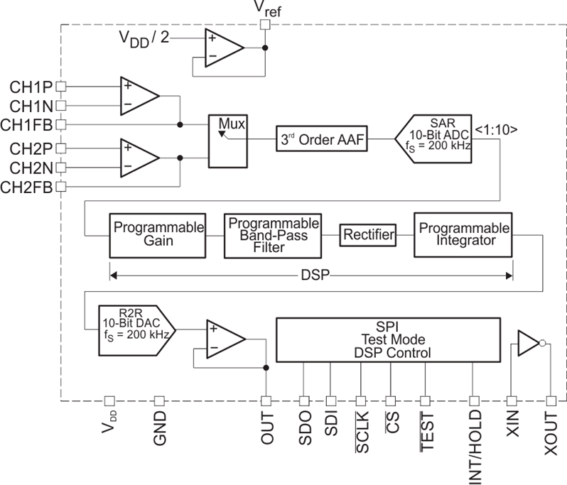
The TPIC8101 is a dual-channel signal processing IC for detection of premature
detonation in combustion engine. The two sensor channels are selectable through the SPI bus. The
knock sensor typically provides an electrical signal to the amplifier inputs. The sensed signal is
processed through a programmable band-pass filter to extract the frequency of interest (engine
knock or ping signals). The band-pass filter eliminates any engine background noise associated with
combustion. The engine background noise is typically low in amplitude compared to the predetonation
noise. The detected signal is full-wave rectified and integrated by use of the INT/HOLD signal.
The digital output from the integration stage is either converted to an analog signal, passed
through an output buffer, or be read directly by the SPI.This analog buffered output may be interfaced to an A/D converter and read by the
microprocessor. The digital output may be directly interfaced to the microprocessor. The data from the A/D enables the system to analyze the amount of retard timing for the
next spark ignition timing cycle. With the microprocessor closed-loop system, advancing and
retarding the spark timing optimizes the load/RPM conditions for a particular engine (data stored
in RAM).
TPIC8101DWR 数据手册
TPIC8101DWR 电路图