TLV5630IPWR 供应商
-
TLV5630IPWR
品牌:TI 封装/批号:原厂原装/22+ -
TLV5630IPWR
品牌:TI(德州仪器) 封装/批号:TSSOP-20/2022+ -
TLV5630IPWR
品牌: 封装/批号:/23+
TLV5630IPWR 属性参数
- 产品培训模块:Data Converter Basics
- 标准包装:2,000
- 类别:集成电路 (IC)
- 家庭:数据采集 - 数模转换器
- 系列:-
- 设置时间:3µs
- 位数:12
- 数据接口:串行
- 转换器数目:8
- 电压电源:模拟和数字
- 功率耗散(最大):48mW
- 工作温度:-40°C ~ 85°C
- 安装类型:表面贴装
- 封装/外壳:20-TSSOP(0.173",4.40mm 宽)
- 供应商设备封装:20-TSSOP
- 包装:带卷 (TR)
- 输出数目和类型:8 电压,单极
- 采样率(每秒):283k
产品特性
- Eight Voltage Output DACs in One Package TLV5630 . . .12-Bit TLV5631 . . .10-Bit TLV5632 . . .8-Bit 1 µs in Fast Mode3 µs in Slow Mode
- TLV5630 . . .12-Bit
- TLV5631 . . .10-Bit
- TLV5632 . . .8-Bit
- 1 µs in Fast Mode
- 3 µs in Slow Mode
- Programmable Settling Time vs Power Consumption 1 µs in Fast Mode3 µs in Slow Mode18 mW in Slow Mode at 3 V48 mW in Fast Mode at 3 V
- 1 µs in Fast Mode
- 3 µs in Slow Mode
- 18 mW in Slow Mode at 3 V
- 48 mW in Fast Mode at 3 V
- Compatible With TMS320 and SPI Serial Ports
- Monotonic Over Temperature
- Low Power Consumption: 18 mW in Slow Mode at 3 V48 mW in Fast Mode at 3 V
- 18 mW in Slow Mode at 3 V
- 48 mW in Fast Mode at 3 V
- Power-Down Mode
- Internal Reference
- Data Output for Daisy-Chaining
- APPLICATIONSDigital Servo Control LoopsDigital Offset and Gain AdjustmentIndustrial Process ControlMachine and Motion Control DevicesMass Storage Devices
- Digital Servo Control Loops
- Digital Offset and Gain Adjustment
- Industrial Process Control
- Machine and Motion Control Devices
- Mass Storage Devices
产品概述
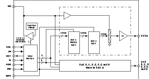
The TLV5630, TLV5631, and TLV5632 are pin-compatible,
eight-channel, 12-/10-/8-bit voltage output DACs each with a flexible serial
interface. The serial interface allows glueless interface to TMS320 and SPI,
QSPI, and Microwire serial ports. It is programmed with a 16-bit serial string
containing 4 control and 12 data bits.Additional features are a power-down mode, an
LDAC input for simultaneous update of all
eight DAC outputs, and a data output which can be used to cascade multiple
devices, and an internal programmable band-gap reference.The resistor string output voltage is buffered by a
rail-to-rail output amplifier with a programmable settling time to allow the
designer to optimize speed vs power dissipation. The buffered, high-impedance
reference input can be connected to the supply voltage.Implemented with a CMOS process, the DACs are designed for
single-supply operation from 2.7 V to 5.5 V, and can operate on two separate analog and digital power supplies. The devices are available in
20-pin SOIC and TSSOP packages.
TLV5630IPWR 电路图