TLV5619QDWREP 供应商
-
TLV5619QDWREP
品牌:TI 封装/批号:原厂原装/22+ -
TLV5619QDWREP
品牌:TI 封装/批号:SOIC20/4 -
TLV5619QDWREP
品牌:TI(德州仪器) 封装/批号:SOIC-20/2022+ -
TLV5619QDWREP
品牌:TI 封装/批号:/05+ -
TLV5619QDWREP
品牌:TI 封装/批号:SOP/23+
TLV5619QDWREP 属性参数
- 产品培训模块:Data Converter Basics
- 标准包装:1
- 类别:集成电路 (IC)
- 家庭:数据采集 - 数模转换器
- 系列:-
- 设置时间:1µs
- 位数:12
- 数据接口:并联
- 转换器数目:1
- 电压电源:单电源
- 功率耗散(最大):8mW
- 工作温度:-40°C ~ 125°C
- 安装类型:表面贴装
- 封装/外壳:20-SOIC(0.295",7.50mm 宽)
- 供应商设备封装:20-SOIC
- 包装:®
- 输出数目和类型:1 电压,单极
- 采样率(每秒):480k
- 配用:296-10736-ND - EVAL MOD FOR TLV5619-TLV5639
- 其它名称:296-18148-6
产品特性
- Controlled Baseline One Assembly/Test Site, One Fabrication Site
- One Assembly/Test Site, One Fabrication Site
- Extended Temperature Performance of –40°C to 125°C
- Enhanced Diminishing Manufacturing Sources (DMS) Support
- Enhanced Product Change Notification
- Qualification Pedigree
- Single Supply 2.7-V to 5.5-V Operation
- ±0.4 LSB Differential Nonlinearity (DNL), ±1.5 LSB Integral Nonlinearity (INL)
- 12-Bit Parallel Interface
- Compatible With TMS320 DSP
- Internal Power On Reset
- Settling Time 1 µs Typ
- Low Power Consumption: 8 mW for 5-V Supply 4.3 mW for 3-V Supply
- 8 mW for 5-V Supply
- 4.3 mW for 3-V Supply
- Reference Input Buffers
- Voltage Output
- Monotonic Over Temperature
- Asynchronous Update
- applications Battery Powered Test Instruments Digital Offset and Gain Adjustment Battery Operated/Remote Industrial Controls Machine and Motion Control Devices Cordless and Wireless Telephones Speech Synthesis Communication Modulators Arbitrary Waveform Generation
- Battery Powered Test Instruments
- Digital Offset and Gain Adjustment
- Battery Operated/Remote Industrial Controls
- Machine and Motion Control Devices
- Cordless and Wireless Telephones
- Speech Synthesis
- Communication Modulators
- Arbitrary Waveform Generation
产品概述
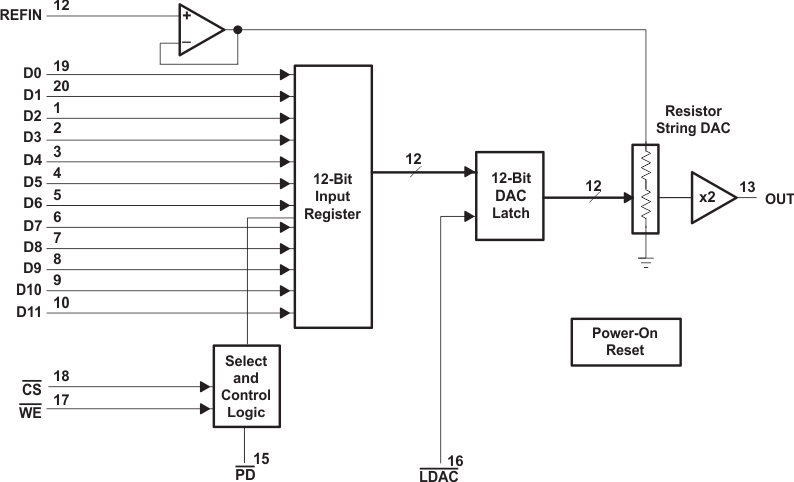
The TLV5619 is a 12-bit voltage output DAC with a microprocessor and TMS320 compatible parallel interface. The 12 data bits are double buffered so that the output can be updated asynchronously using the LDAC\ pin. During normal operation, the device dissipates 8 mW at a 5-V supply and 4.3 mW at a 3-V supply. The power consumption can be lowered to 50 nW by setting the DAC to power-down mode.The output voltage is buffered by a ×2 gain rail-to-rail amplifier, which features a Class A output stage to improve stability and reduce settling time.
TLV5619QDWREP 数据手册
TLV5619QDWREP 电路图