TLV171QDBVRQ1 供应商
-
TLV171QDBVRQ1
品牌:TI 封装/批号:原厂原装/22+ -
TLV171QDBVRQ1
品牌:TI(德州仪器) 封装/批号:SOT-23-5/2022+ -
TLV171QDBVRQ1
品牌:TI 封装/批号:/21+/22+ -
TLV171QDBVRQ1
品牌: 封装/批号:TSSOP/23+
TLV171QDBVRQ1 属性参数
- 现有数量:0现货查看交期
- 价格:1 : ¥11.85000剪切带(CT)3,000 : ¥5.37811卷带(TR)
- 系列:Automotive, AEC-Q100
- 包装:卷带(TR)剪切带(CT)? 得捷定制卷带
- 产品状态:在售
- 放大器类型:通用
- 电路数:1
- 输出类型:满摆幅
- 压摆率:1.5V/μs
- 增益带宽积:3 MHz
- -3db 带宽:-
- 电流 - 输入偏置:10 pA
- 电压 - 输入补偿:750 μV
- 电流 - 供电:525μA
- 电流 - 输出/通道:25 mA
- 电压 - 跨度(最小值):4.5 V
- 电压 - 跨度(最大值):36 V
- 工作温度:-40°C ~ 125°C
- 安装类型:表面贴装型
- 封装/外壳:SC-74A,SOT-753
- 供应商器件封装:SOT-23-5
产品特性
- Qualified for Automotive Applications
- AEC-Q100 Test Guidance With the Following Results:Device Temperature Grade 1: –40°C to +125°C Ambient Operating TemperatureDevice HBM ESD Classification Level: Level 3A for TLV171-Q1 and TLV2171-Q1 Level 2 for TLV4171-Q1Device CDM ESD Classification Level Level C4A for TLV171-Q1 Level C6 for TLV2171-Q1and TLV4171-Q1
- Device Temperature Grade 1: –40°C to +125°C Ambient Operating Temperature
- Device HBM ESD Classification Level: Level 3A for TLV171-Q1 and TLV2171-Q1 Level 2 for TLV4171-Q1
- Level 3A for TLV171-Q1 and TLV2171-Q1
- Level 2 for TLV4171-Q1
- Device CDM ESD Classification Level Level C4A for TLV171-Q1 Level C6 for TLV2171-Q1and TLV4171-Q1
- Level C4A for TLV171-Q1
- Level C6 for TLV2171-Q1and TLV4171-Q1
- Supply Range: Single-Supply: 4.5 V to 36 V Dual-Supply ±2.25 V to ±18 V
- Single-Supply: 4.5 V to 36 V
- Dual-Supply ±2.25 V to ±18 V
- Low Noise: 16 nV/√Hz at 1 kHz
- Low Offset Drift: ±1 µV/°C (Typical)
- Input Range Includes Negative Supply
- Input Range Operates to Positive Supply With Reduced Performance
- Rail-to-Rail Output
- Gain Bandwidth: 3 MHz
- Low Quiescent Current: 525 µA per Amplifier
- Common-Mode Rejection: 120 dB (Typical)
- Low Input Bias Current: 10 pA
产品概述
The TLVx171-Q1
family of devices is a 36-V,
single-supply, low-noise operational amplifier (op amp) with the ability to operate on
supplies ranging from 4.5 V
(± 2.25 V) to 36 V (±18 V). This
series is available in multiple packages and offers low offset, drift, and low quiescent current.
The single, dual, and quad versions all have identical specifications for maximum design
flexibility.Unlike most op amps, which are specified at only one supply voltage, the
TLVx171-Q1 family of devices
is specified from 4.5 V to 36 V.
Input signals beyond the supply rails do not cause phase reversal.
The TLVx171-Q1 family
of devices is stable with capacitive loads up to 300 pF. The input can operate 100 mV below the
negative rail and within 2 V of the top rail during normal operation. The device can operate with
full rail-to-rail input 100 mV beyond the top rail, but with reduced performance within 2 V of the
top rail.The TLVx171-Q1 op
amp family is specified from –40°C to +125°C.
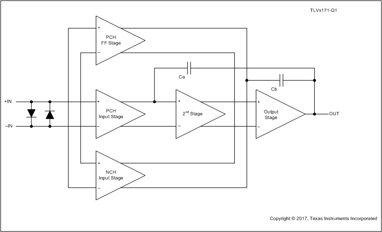
TLV171QDBVRQ1 电路图