TLV1548QDBRQ1 供应商
-
TLV1548QDBRQ1
品牌:TI 封装/批号:原厂原装/22+ -
TLV1548QDBRQ1
品牌:TI(德州仪器) 封装/批号:SSOP-20/2022+
TLV1548QDBRQ1 属性参数
- 产品培训模块:Data Converter Basics
- 标准包装:1
- 类别:集成电路 (IC)
- 家庭:数据采集 - 模数转换器
- 系列:-
- 位数:10
- 采样率(每秒):87k
- 数据接口:DSP,串行,SPI?
- 转换器数目:1
- 功率耗散(最大):785mW
- 电压电源:单电源
- 工作温度:-40°C ~ 125°C
- 安装类型:表面贴装
- 封装/外壳:20-SSOP(0.209",5.30mm 宽)
- 供应商设备封装:20-SSOP
- 包装:®
- 输入数目和类型:8 个单端,单极
- 其它名称:296-16956-6
产品特性
- Qualified for Automotive Applications
- ESD Protection Exceeds 2000 V Per MIL-STD-883, Method 3015; Exceeds 200 V Using Machine Model (C = 200 pF, R = 0)
- Conversion Time ≤ 10 µs
- 10-Bit-Resolution ADC
- Programmable Power-Down Mode . . . 1 µA
- Wide Range Single-Supply Operation of 2.7 V dc to 5.5 V dc
- Analog Input Range of 0 V to VCC
- Built-in Analog Multiplexer with 8 Analog Input Channels
- TMS320 DSP and Microprocessor SPI and QSPI Compatible Serial Interfaces
- End-of-Conversion (EOC) Flag
- Inherent Sample-and-Hold Function
- Built-In Self-Test Modes
- Programmable Power and Conversion Rate
- Asynchronous Start of Conversion for Extended Sampling
- Hardware I/O Clock Phase Adjust Input
产品概述
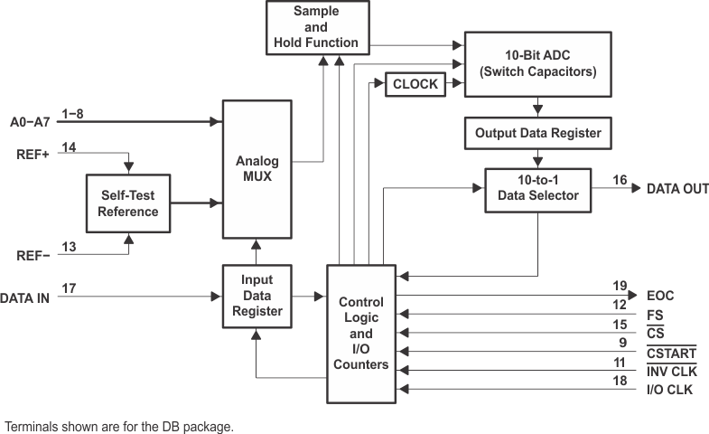
The TLV1548 is a CMOS 10-bit switched-capacitor successive-approximation (SAR) analog-to-digital (A/D) converter. The device has a chip select (CS), input-output clock (I/O CLK), data input (DATA IN) and serial data output (DATA OUT) that provides a direct 4-wire synchronous serial peripheral interface (SPI™, QSPI™) port of a host microprocessor. When interfacing with a TMS320 DSP, an additional frame sync signal (FS) indicates the start of a serial data frame. The device allows high-speed data transfers from the host. The INV CLK\ input provides further timing flexibility for the serial interface.In addition to a high-speed converter and versatile control capability, the device has an on-chip 11-channel multiplexer that can select any one of eight analog inputs or any one of three internal self-test voltages. The sample-and-hold function is automatic except for the extended sampling cycle, where the sampling cycle is started by the falling edge of asynchronous CSTART. At the end of the A/D conversion, the end-of-conversion (EOC) output goes high to indicate that the conversion is complete. The TLV1548 is designed to operate with a wide range of supply voltages with very low power consumption. The power saving feature is further enhanced with a software-programmed power-down mode and conversion rate. The converter incorporated in the device features differential high-impedance reference inputs that facilitate ratiometric conversion, scaling, and isolation of analog circuitry from logic and supply noise. A switched-capacitor design allows low-error conversion over the full operating temperature range.The TLV1548 has eight analog input channels. The TLV1548Q is characterized for operation over the full automotive temperature range of –40°C to 125°C.
TLV1548QDBRQ1 电路图