TLC7528CN 供应商
TLC7528CN 属性参数
- 产品培训模块:Data Converter Basics
- 标准包装:20
- 类别:集成电路 (IC)
- 家庭:数据采集 - 数模转换器
- 系列:-
- 设置时间:100ns
- 位数:8
- 数据接口:并联
- 转换器数目:2
- 电压电源:单电源
- 功率耗散(最大):20mW
- 工作温度:0°C ~ 70°C
- 安装类型:通孔
- 封装/外壳:20-DIP(0.300",7.62mm)
- 供应商设备封装:20-PDIP
- 包装:管件
- 输出数目和类型:2 电流,双极
- 采样率(每秒):-
- 其它名称:296-1871296-1871-5
产品特性
- Easily Interfaced to Microprocessors
- On-Chip Data Latches
- Monotonic Over the Entire A/D Conversion Range
- Interchangeable With Analog Devices AD7528 and PMI PM-7528
- Fast Control Signaling for Digital Signal Processor (DSP) Applications Including Interface With TMS320
- Voltage-Mode Operation
- CMOS Technology
产品概述
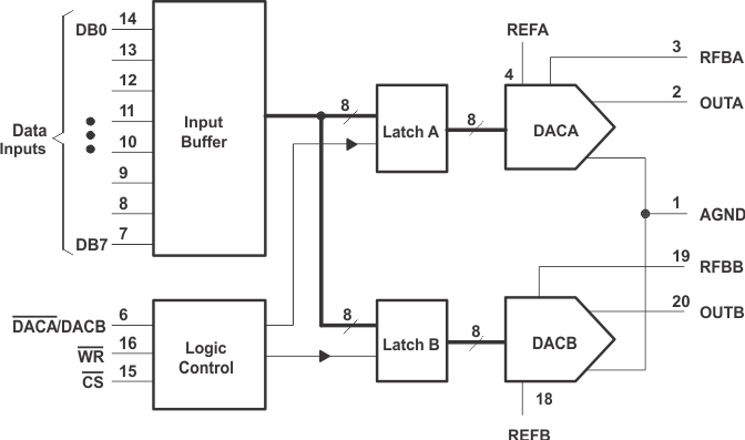
The TLC7528C, TLC7528E, and TLC7528I are dual, 8-bit, digital-to-analog converters (DACs) designed with separate on-chip data latches and feature exceptionally close DAC-to-DAC matching. Data is transferred to either of the two DAC data latches through a common, 8-bit, input port. Control input DACA/DACB determines which DAC is to be loaded. The load cycle of these devices is similar to the write cycle of a random-access memory, allowing easy interface to most popular microprocessor buses and output ports. Segmenting the high-order bits minimizes glitches during changes in the most significant bits, where glitch impulse is typically the strongest.These devices operate from a 5V to 15V power supply and dissipates less than 15 mW (typical). The 2- or 4-quadrant multiplying makes these devices a sound choice for many microprocessor-controlled gain-setting and signal-control applications. It can be operated in voltage mode, which produces a voltage output rather than a current output. Refer to the typical application information in this data sheet.The TLC7528C is characterized for operation from 0°C to 70°C. The TLC7528I is characterized for operation from -25°C to 85°C. The TLC7528E is characterized for operation from -40°C to 85°C.
TLC7528CN 数据手册
TLC7528CN 电路图