TLC59212IPWR 供应商
-
TLC59212IPWR
品牌:TI 封装/批号:原厂原装/22+ -
TLC59212IPWR
品牌:TI(德州仪器) 封装/批号:TSSOP-20/2022+
TLC59212IPWR 属性参数
- 标准包装:1
- 类别:集成电路 (IC)
- 家庭:逻辑 - 触发器
- 系列:-
- 功能:主复位
- 类型:D 型总线
- 输出类型:反相
- 元件数:1
- 每个元件的位元数:8
- 频率 - 时钟:1MHz
- 延迟时间 - 传输:70ns
- 触发器类型:正边沿
- 输出电流高,低:-,40mA
- 电源电压:4.5 V ~ 5.5 V
- 工作温度:-40°C ~ 85°C
- 安装类型:表面贴装
- 封装/外壳:20-TSSOP(0.173",4.40mm 宽)
- 包装:®
- 其它名称:296-25405-6
产品特性
- LBC3S (Lin BiCMOS) Process
- High Voltage Output (VOUT = 24 V)
- Output Current (IOL Maximum = 40 mA)
- Latch-Up Performance Exceeds 250 mA Per JEDEC Standard JESD-17
- ESD Protection Exceeds JESD 22 2000-V Human Body Model (A114-A) 200-V Machine Model (A115-A) 1000-V Charged Device Model (C101)
- 2000-V Human Body Model (A114-A)
- 200-V Machine Model (A115-A)
- 1000-V Charged Device Model (C101)
产品概述
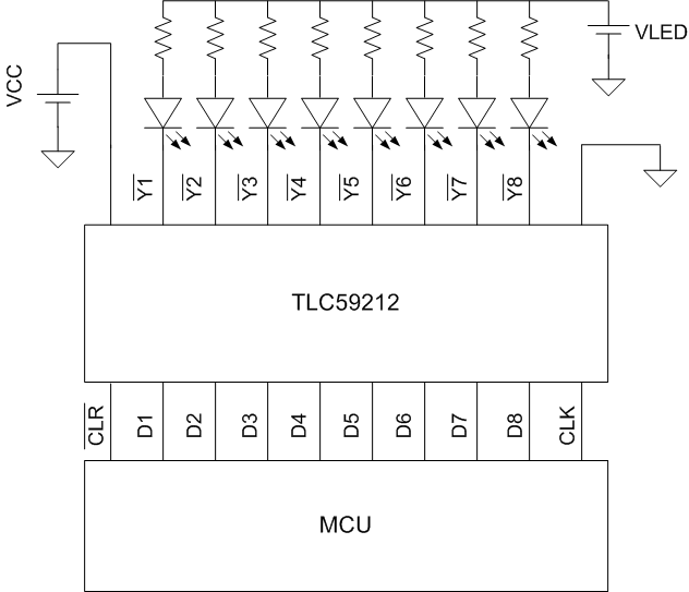
The TLC59212 device is an 8-bit open-collector driver with latch designed for 5-V
VCC operation.These circuits are positive-edge-triggered D-type flip-flops with a direct clear
(CLR) input. Information at the data (D) input meeting the setup time
requirements is transferred to the Y output on the positive-going edge of
the clock (CLK) pulse. Clock triggering occurs at a particular voltage level and is not directly
related to the transition time of the positive-going pulse. When CLK is at either the high or low
level, the D-input has no effect at the output.The TLC59212 is characterized for operation from –40°C to 85°C.
TLC59212IPWR 电路图