TLC3702QDRQ1 供应商
-
TLC3702QDRQ1 原装现货
品牌:TI 封装/批号:SOP/21+/22+ -
TLC3702QDRQ1
品牌:TI 封装/批号:原厂原装/22+ -
TLC3702QDRQ1
品牌:TI/德州仪器 封装/批号:21+/SOP8 -
TLC3702QDRQ1
品牌:TI(德州仪器) 封装/批号:SOIC-8/2022+ -
TLC3702QDRQ1
品牌:TI 封装/批号:/21+ -
TLC3702QDRQ1
品牌:TLC3702QDRQ1 封装/批号:TI/连可连代销V
TLC3702QDRQ1 属性参数
- 标准包装:1
- 类别:集成电路 (IC)
- 家庭:线性 - 比较器
- 系列:LinCMOS™
- 类型:通用
- 元件数:2
- 输出类型:CMOS,推挽式,TTL
- 电压 - 电源,单路/双路(±):4 V ~ 16 V
- 电压 - 输入偏移(最小值):5mV @ 10V
- 电流 - 输入偏压(最小值):5pA @ 5V
- 电流 - 输出(标准):20mA
- 电流 - 静态(最大值):90µA
- CMRR, PSRR(标准):84dB CMRR
- 传输延迟(最大):4.5µs
- 磁滞:-
- 工作温度:-40°C ~ 125°C
- 封装/外壳:8-SOIC(0.154",3.90mm 宽)
- 安装类型:表面贴装
- 包装:®
- 其它名称:296-18903-6
产品特性
- Qualified for Automotive Applications
- AEC-Q100 Qualified With the Following Results: Device Temperature Grade 1: –40°C to +125°C Ambient Operating Temperature Range Device HBM ESD Classification Level H2 Devce CDM ESD Classification Level C4B
- Device Temperature Grade 1: –40°C to +125°C Ambient Operating Temperature Range
- Device HBM ESD Classification Level H2
- Devce CDM ESD Classification Level C4B
- Push-Pull CMOS Output Drives Capacitive Loads Without Pullup Resistor, IO = ± 8 mA
- Very Low Power…100 µW Typical at 5 V
- Fast Response Time… tPLH = 2.7 µs Typical With 5-mV Overdrive
- Single-Supply Operation…3 V to 16 V
- On-Chip ESD Protection
产品概述
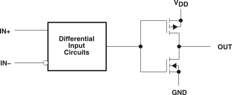
The TLC3702-Q1 consists of two independent micro-power voltage comparators. Compared to
similar devices, the TLC3702-Q1 uses one-twentieth of the power for similar response times. This
allows the device to react quickly to fast changing signals while extending the battery
life.The push-pull CMOS output stage drives capacitive loads directly without a power
consuming pullup resistor to achieve the stated response time. Eliminating the pullup resistor not
only reduces power dissipation but also saves board space and component cost. Additionally, the
output stage is fully compatible with all TTL and CMOS logic requirements.Texas Instruments’ LinCMOS™ process offers superior
analog performance versus standard CMOS processes. Along with the standard CMOS advantages of low
power without sacrificing speed, high input impedance and low bias currents, the LinCMOS process
offers extremely stable input/offset voltages with large differential input voltages. This
characteristic makes it possible to build reliable CMOS comparators.The TLC3702-Q1 has a wide supply range from 3 V to 16 V, allowing design flexibility. The
voltage range also allows the device to handle start-stop applications and be connected directly to
a standard 12-V battery. All of these features make the TLC3702-Q1 suitable for HEV/EV and
powertrain system such as transmission control unit (TCU) and engine control.
TLC3702QDRQ1 电路图