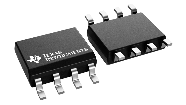
TLC071CDR 供应商
TLC071CDR 属性参数
- 标准包装:1
- 类别:集成电路 (IC)
- 家庭:Linear - Amplifiers - Instrumentation, OP Amps, Buffer Amps
- 系列:-
- 放大器类型:通用
- 电路数:1
- 输出类型:-
- 转换速率:19 V/µs
- 增益带宽积:10MHz
- -3db带宽:-
- 电流 - 输入偏压:1.5pA
- 电压 - 输入偏移:390µV
- 电流 - 电源:2.1mA
- 电流 - 输出 / 通道:57mA
- 电压 - 电源,单路/双路(±):4.5 V ~ 16 V,±2.25 V ~ 8 V
- 工作温度:0°C ~ 70°C
- 安装类型:表面贴装
- 封装/外壳:8-SOIC(0.154",3.90mm 宽)
- 供应商设备封装:8-SOIC
- 包装:®
- 其它名称:296-31953-6
产品特性
- Wide Bandwidth . . . 10 MHz
- High Output Drive IOH . . . 57 mA at VDD – 1.5 V IOL . . . 55 mA at 0.5 V
- IOH . . . 57 mA at VDD – 1.5 V
- IOL . . . 55 mA at 0.5 V
- High Slew Rate SR+ . . . 16 V/µs SR– . . . 19 V/µs
- SR+ . . . 16 V/µs
- SR– . . . 19 V/µs
- Wide Supply Range . . . 4.5 V to 16 V
- Supply Current . . . 1.9 mA/Channel
- Ultralow Power Shutdown Mode IDD . . . 125 µA/Channel
- IDD . . . 125 µA/Channel
- Low Input Noise Voltage . . . 7 nV√Hz
- Input Offset Voltage . . . 60 µV
- Ultra-Small Packages
- 8 or 10 Pin MSOP (TLC070/1/2/3)
产品概述
The first members of TI’s new BiMOS general-purpose operational amplifier family are the TLC07x. The BiMOS family concept is simple: provide an upgrade path for BiFET users who are moving away from dual-supply to single-supply systems and demand higher AC and dc performance. With performance rated from 4.5 V to 16 V across commercial (0°C to 70°C) and an extended industrial temperature range (–40°C to 125°C), BiMOS suits a wide range of audio, automotive, industrial and instrumentation applications. Familiar features like offset nulling pins, and new features like MSOP PowerPAD. packages and shutdown modes, enable higher levels of performance in a variety of applications.Developed in TI’s patented LBC3 BiCMOS process, the new BiMOS amplifiers combine a very high input impedance low-noise CMOS front end with a high-drive bipolar output stage, thus providing the optimum performance features of both. AC performance improvements over the TL07x BiFET predecessors include a bandwidth of 10 MHz (an increase of 300%) and voltage noise of 7 nV/√Hz (an improvement of 60%). DC improvements include a factor of 4 reduction in input offset voltage down to 1.5 mV (maximum) in the standard grade, and a power supply rejection improvement of greater than 40 dB to 130 dB. Added to this list of impressive features is the ability to drive ±50-mA loads comfortably from an ultrasmall-footprint MSOP PowerPAD package, which positions the TLC07x as the ideal high-performance general-purpose operational amplifier family.
