THS1206MDAREP 供应商
-
THS1206MDAREP
品牌:Texas Instruments 封装/批号:TSSOP32/21+ -
THS1206MDAREP
品牌:TI(德州仪器) 封装/批号:TSSOP-32/2022+
THS1206MDAREP 属性参数
- 制造商:Texas Instruments
- 产品种类:ADC(模数转换器)
- 转换器数量:1
- ADC 输入端数量:4, 2
- 结构:Pipelined
- 转换速率:6000 KSPs
- 分辨率:12 bit
- 输入类型:Voltage
- 接口类型:Parallel
- 信噪比:69 dB
- 电压参考:Internal, External
- Supply Voltage - Max:5.25 V
- Supply Voltage - Min:4.75 V
- 最大功率耗散:216 mW
- 最大工作温度:+ 125 C
- 安装风格:SMD/SMT
- 封装 / 箱体:TSSOP-32
- 封装:Reel
- 最小工作温度:- 55 C
- 工作电源电压:5 V
- 工厂包装数量:2000
产品特性
- Controlled Baseline One Assembly/Test Site, One Fabrication Site
- One Assembly/Test Site, One Fabrication Site
- Extended Temperature Performance of –55°C to 125°C
- Enhanced Diminishing Manufacturing Sources (DMS) Support
- Enhanced Product Change Notification
- Qualification Pedigree
- High-Speed 6 MSPS ADC
- 4 Single-Ended or 2 Differential Inputs
- Simultaneous Sampling of 4 Single-Ended Signals or 2 Differential Signals or Combination of Both
- Differential Nonlinearity Error: ±1 LSB
- Integral Nonlinearity Error: ±1.8 LSB
- Signal-to-Noise and Distortion Ratio: 68 dB at fI = 2 MHz
- Auto-Scan Mode for 2, 3, or 4 Inputs
- 3-V or 5-V Digital Interface Compatible
- Low Power: 216 mW Max
- 5-V Analog Single Supply Operation
- Internal Voltage References . . . 50 PPM/°C and ±5% Accuracy
- Glueless DSP Interface
- Parallel µC/DSP Interface
- Integrated FIFO
- Available in TSSOP Package
- applications Radar Applications Communications Control Applications High-Speed DSP Front-End Selected Military Applications
- Radar Applications
- Communications
- Control Applications
- High-Speed DSP Front-End
- Selected Military Applications
产品概述
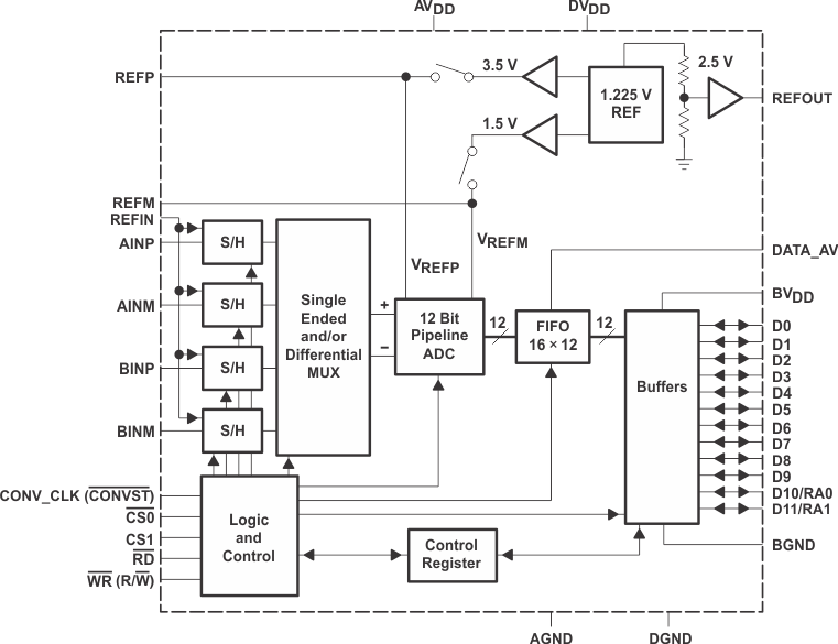
The THS1206 is a CMOS, low-power, 12-bit, 6 MSPS analog-to-digital converter (ADC). The speed, resolution, bandwidth, and single-supply operation are suited for applications in radar, imaging, high-speed acquisition, and communications. A multistage pipelined architecture with output error correction logic provides for no missing codes over the full operating temperature range. Internal control registers are used to program the ADC into the desired mode. The THS1206 consists of four analog inputs, which are sampled simultaneously. These inputs can be selected individually and configured to single-ended or differential inputs. An integrated 16 word deep FIFO allows the storage of data in order to take the load off of the processor connected to the ADC. Internal reference voltages for the ADC (1.5 V and 3.5 V) are provided.An external reference can also be chosen to suit the dc accuracy and temperature drift requirements of the application. Two different conversion modes can be selected. In single conversion mode, a single and simultaneous conversion of up to four inputs can be initiated by using the single conversion start signal (CONVST)\. The conversion clock in single conversion mode is generated internally using a clock oscillator circuit. In continuous conversion mode, an external clock signal is applied to the CONV_CLK input of the THS1206. The internal clock oscillator is switched off in continuous conversion mode.
THS1206MDAREP 数据手册
THS1206MDAREP 电路图