SN75108ADR 供应商
-
SN75108ADR
品牌:TI 封装/批号:原厂原装/22+ -
SN75108ADR
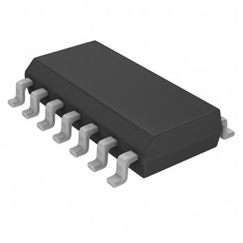
品牌:TI(德州仪器) 封装/批号:SOIC-14/2022+
SN75108ADR 属性参数
- 标准包装:2,500
- 类别:集成电路 (IC)
- 家庭:接口 - 驱动器,接收器,收发器
- 系列:-
- 类型:线路接收器
- 驱动器/接收器数:0/2
- 规程:-
- 电源电压:±4.75 V ~ 5.25 V
- 安装类型:表面贴装
- 封装/外壳:14-SOIC(0.154",3.90mm 宽)
- 供应商设备封装:14-SOIC
- 包装:带卷 (TR)
产品特性
- High Speed
- Standard Supply Voltage
- Dual Channels
- High Common-Mode Rejection Ratio
- High Input Impedance
- High Input Sensitivity
- Differential Common-Mode Input Voltage Range of ±3 V
- Strobe Inputs for Receiver Selection
- Gate Inputs for Logic Versatility
- TTL Drive Capability
- High dc Noise Margin
- Totem-Pole Outputs
- B Version Has Diode-Protected Input for Power-Off Condition
产品概述
These circuits are TTL-compatible, high-speed line receivers. Each is a monolithic dual circuit featuring two independent channels. They are designed for general use, as well as for such specific applications as data comparators and balanced, unbalanced, and party-line transmission systems. These devices are unilaterally interchangeable with and are replacements for the SN55107, SN75107, and SN75108, but offer diode-clamped strobe inputs to simplify circuit design.
The essential difference between the A and B versions can be seen in the schematics. Input-protection diodes are in series with the collectors of the differential-input transistors of the B versions. These diodes are useful in certain party-line systems that have multiple VCC+ power supplies and can be operated with some of the VCC+ supplies turned off. In such a system, if a supply is turned off and allowed to go to ground, the equivalent input circuit connected to that supply would be as follows:
This would be a problem in specific systems that might have the transmission lines biased to some potential greater than 1.4 V.
The SN55107A is characterized for operation over the full military temperature range of -55°C to 125°C. The SN75107A, SN75107B, and SN75108A are characterized for operation from 0°C to 70°C.
H = high level, L = low level, X = irrelevant