SN74LVC2G00DCUT 供应商
-
SN74LVC2G00DCUT
品牌:TI 封装/批号:原厂原装/22+ -
SN74LVC2G00DCUT
品牌:TI 封装/批号:TSSOP/23+
SN74LVC2G00DCUT 属性参数
- 标准包装:1
- 类别:集成电路 (IC)
- 家庭:逻辑 - 栅极和逆变器
- 系列:74LVC
- 逻辑类型:与非门
- 电路数:2
- 输入数:2
- 特点:-
- 电源电压:1.65 V ~ 5.5 V
- 电流 - 静态(最大值):10µA
- 输出电流高,低:32mA,32mA
- 逻辑电平 - 低:0.7 V ~ 0.8 V
- 逻辑电平 - 高:1.7 V ~ 2 V
- 额定电压和最大 CL 时的最大传播延迟:3.3ns @ 5V,50pF
- 工作温度:-40°C ~ 85°C
- 安装类型:*
- 供应商设备封装:*
- 封装/外壳:*
- 包装:*
- 其它名称:296-32318-6
产品特性
- Available in the Texas Instruments NanoFree™ Package
- Supports 5-V VCC Operation
- Inputs Accept Voltages to 5.5 V
- Max tpd of 4.3 ns at 3.3 V
- Low Power Consumption, 10-µA Max ICC
- ±24-mA Output Drive at 3.3 V
- Typical VOLP (Output Ground Bounce) < 0.8 V at VCC = 3.3 V, TA = 25°C
- Typical VOHV (Output VOH Undershoot) > 2 V at VCC = 3.3 V, TA = 25°C
- Ioff Supports Live Insertion, Partial Power Down Mode, and Back Drive Protection
- Latch-Up Performance Exceeds 100 mA Per JESD 78, Class II
- ESD Protection Exceeds JESD 22 2000-V Human-Body Model 1000-V Charged-Device Model
- 2000-V Human-Body Model
- 1000-V Charged-Device Model
产品概述
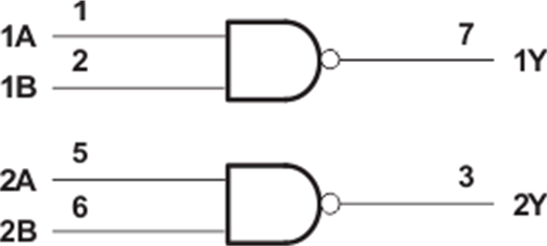
This dual 2-input positive-NAND gate is designed for 1.65-V to 5.5-V
VCC operation.The SN74LVC2G00 device performs the Boolean function Y = A × B or
Y = A + B in positive logic.NanoFree™ package technology is a major breakthrough in IC packaging concepts, using the
die as the package.This device is fully specified for partial-power-down applications using
Ioff. The Ioff circuitry disables the outputs,
preventing damaging current backflow through the device when it is powered down.
SN74LVC2G00DCUT 数据手册
SN74LVC2G00DCUT 电路图