SN74LVC1G97DRLR 供应商
-
SN74LVC1G97DRLR
品牌:TI 封装/批号:原厂原装/22+ -
SN74LVC1G97DRLR
品牌:TI(德州仪器) 封装/批号:SOT-563/2022+ -
SN74LVC1G97DRLR
品牌:TI 封装/批号:/2021+
SN74LVC1G97DRLR 属性参数
- 标准包装:1
- 类别:集成电路 (IC)
- 家庭:逻辑 - 栅极和逆变器 - 多功能,可配置
- 系列:74LVC
- 逻辑类型:可配置多功能
- 电路数:1
- 输入数:3
- 施密特触发器输入:是
- 输出类型:单端
- 输出电流高,低:32mA,32mA
- 电源电压:1.65 V ~ 5.5 V
- 工作温度:-40°C ~ 85°C
- 安装类型:表面贴装
- 封装/外壳:SOT-563,SOT-666
- 供应商设备封装:6-SOT
- 包装:®
- 其它名称:296-18655-6
产品特性
- ESD Protection Exceeds JESD 22 2000-V Human Body Model (A114-A) 200-V Machine Model (A115-A) 1000-V Charged-Device Model (C101)
- 2000-V Human Body Model (A114-A)
- 200-V Machine Model (A115-A)
- 1000-V Charged-Device Model (C101)
- Available in the Texas Instruments NanoFree&traDe; Package
- Supports 5-V VCC Operation
- Inputs Accept Voltages to 5.5 V
- Supports Down Translation to VCC
- Max tpd of 6.3 ns at 3.3 V
- Low Power Consumption, 10-µA Max ICC
- ±24-mA Output Drive at 3.3 V
- Ioff Supports Live Insertion, Partial-Power-Down Mode, and Back-Drive Protection
- Latch-Up Performance Exceeds 100 mA Per JESD 78, Class II
- Choose From Nine Specific Logic Functions
产品概述
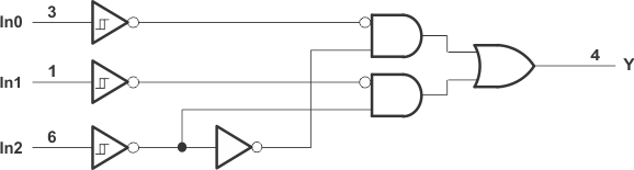
The SN74LVC1G97 device features configurable multiple functions. The output state is
determined by eight patterns of 3-bit input. The user can choose the logic functions MUX, AND, OR,
NAND, NOR, inverter, and noninverter. All inputs can be connected to VCC or
GND.This configurable multiple-function gate is designed for 1.65-V to 5.5-V
VCC operation.This device functions as an independent gate, but because of Schmitt action, it may have
different input threshold levels for positive-going (VT+) and negative-going
(VT–) signals.NanoFree package technology is a major break-through in IC packaging concepts, using the
die as the package.This device is fully specified for partial-power-down applications using
Ioff. The Ioff circuitry disables the outputs,
preventing damaging current backflow through the device when it is powered down.
SN74LVC1G97DRLR 数据手册
SN74LVC1G97DRLR 电路图