SN74LVC1G34DPWR 供应商
-
SN74LVC1G34DPWR
品牌:TI 封装/批号:原厂原装/22+
SN74LVC1G34DPWR 属性参数
- 现有数量:0现货查看交期
- 价格:1 : ¥3.58000剪切带(CT)3,000 : ¥1.01004卷带(TR)
- 系列:74LVC
- 包装:卷带(TR)剪切带(CT)? 得捷定制卷带
- 产品状态:在售
- 逻辑类型:缓冲器,非反向
- 元件数:1
- 每个元件位数:1
- 输入类型:-
- 输出类型:推挽式
- 电流 - 输出高、低:32mA,32mA
- 电压 - 供电:1.65V ~ 5.5V
- 工作温度:-40°C ~ 125°C(TA)
- 安装类型:表面贴装型
- 封装/外壳:4-XFDFN 裸露焊盘
- 供应商器件封装:4-X2SON(0.8x0.8)
产品特性
- Available in the Ultra Small 0.64-mm2 Package (DPW) with 0.5-mm Pitch
- Supports 5-V VCC Operation
- Inputs Accept Voltages to 5.5 V
- Provides Down Translation to VCC
- Max tpd of 3.5 ns at 3.3 V
- Low Power Consumption, 1-µA Max ICC
- ±24-mA Output Drive at 3.3 V
- Ioff Supports Live Insertion, Partial Power Down Mode, and Back Drive Protection
- Latch-Up Performance Exceeds 100 mA Per JESD 78, Class II
- ESD Protection Exceeds JESD 22 2000-V Human-Body Model (A114-A) 200-V Machine Model (A115-A) 1000-V Charged-Device Model (C101)
- 2000-V Human-Body Model (A114-A)
- 200-V Machine Model (A115-A)
- 1000-V Charged-Device Model (C101)
产品概述
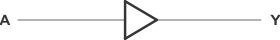
This single buffer gate is designed for 1.65-V to 5.5-V VCC
operation.The SN74LVC1G34 device performs the Boolean function Y = A in positive logic. The CMOS device has high output drive while maintaining low static power dissipation
over a broad VCC Operating range.The SN74LVC1G34 is available in a variety of packages, including the ultra-small DPW
package with a body size of 0.8 mm × 0.8 mm.
SN74LVC1G34DPWR 数据手册
SN74LVC1G34DPWR 电路图