SN74LVC1G06YZVR 供应商
-
SN74LVC1G06YZVR
品牌:TI 封装/批号:原厂原装/22+ -
SN74LVC1G06YZVR
品牌:TI(德州仪器) 封装/批号:DSBGA-4(0.88x0.88)/2022+
SN74LVC1G06YZVR 属性参数
- 标准包装:1
- 类别:集成电路 (IC)
- 家庭:逻辑 - 栅极和逆变器
- 系列:74LVC
- 逻辑类型:逆变器,缓冲器
- 电路数:1
- 输入数:1
- 特点:开路漏极
- 电源电压:1.65 V ~ 5.5 V
- 电流 - 静态(最大值):10µA
- 输出电流高,低:-,32mA
- 逻辑电平 - 低:0.7 V ~ 0.8 V
- 逻辑电平 - 高:1.7 V ~ 2 V
- 额定电压和最大 CL 时的最大传播延迟:3ns @ 5V,50pF
- 工作温度:-40°C ~ 85°C
- 安装类型:表面贴装
- 供应商设备封装:4-DSBGA(0.9x0.9)
- 封装/外壳:4-XFBGA,DSBGA
- 包装:®
- 其它名称:296-21056-6
产品特性
- ESD Protection Exceeds JESD 22 2000-V Human Body Model (A114-A) 200-V Machine Model (A115-A) 1000-V Charged-Device Model (C101)
- 2000-V Human Body Model (A114-A)
- 200-V Machine Model (A115-A)
- 1000-V Charged-Device Model (C101)
- Available in the Texas Instruments NanoFree™ Package
- Supports 5-V VCC Operation
- Input and Open-Drain Output Accept Voltages up to 5.5 V
- Maximum tpd of 4.5 ns at 3.3 V at 125°C
- Low Power Consumption, 10-µA Maximum ICC
- ±24-mA Output Drive at 3.3 V for open-drain devices
- Ioff Supports Partial-Power-Down Mode and Back-Drive Protection
- Latch-Up Performance Exceeds 100 mA Per JESD 78, Class II
- Can Be Used For Up or Down Translation
- Schmitt Trigger Action on All Ports
产品概述
This single inverter buffer and driver is designed for 1.65-V to 5.5-V
VCC operation.NanoFree package technology is a major breakthrough in IC packaging concepts, using the
die as the package.The output of the SN74LVC1G06 device is open-drain and can be connected to other
open-drain outputs to implement active-low wired-OR or active-high wired-AND functions. The maximum
sink current is 32 mA.This device is fully specified for partial-power-down applications using
Ioff.The Ioff circuitry disables the outputs when the
device is powered down. This inhibits current backflow into the device which prevents damage to the
device.
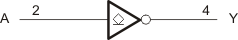
SN74LVC1G06YZVR 电路图