SN74LVC1G04QDBVRQ1 供应商
-
SN74LVC1G04QDBVRQ1
品牌:TI 封装/批号:原厂原装/22+ -
SN74LVC1G04QDBVRQ1
品牌:ti 封装/批号:/02+ -
SN74LVC1G04QDBVRQ1
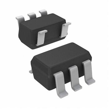
品牌:TI(德州仪器) 封装/批号:SOT-23-5/2022+ -
SN74LVC1G04QDBVRQ1
品牌:TI 封装/批号:TSSOP/23+
SN74LVC1G04QDBVRQ1 属性参数
- 标准包装:1
- 类别:集成电路 (IC)
- 家庭:逻辑 - 栅极和逆变器
- 系列:74LVC
- 逻辑类型:逆变器,缓冲器
- 电路数:1
- 输入数:1
- 特点:-
- 电源电压:1.65 V ~ 5.5 V
- 电流 - 静态(最大值):10µA
- 输出电流高,低:32mA,32mA
- 逻辑电平 - 低:0.7 V ~ 0.8 V
- 逻辑电平 - 高:1.7 V ~ 2 V
- 额定电压和最大 CL 时的最大传播延迟:3.7ns @ 5V,50pF
- 工作温度:-40°C ~ 125°C
- 安装类型:表面贴装
- 供应商设备封装:SOT-23-5
- 封装/外壳:SC-74A,SOT-753
- 包装:®
- 其它名称:296-26588-6
产品特性
- Qualified for Automotive Applications
- AEC-Q100 Qualified with the Following Results Device Temperature Grade 1: –40°C to 125°C Ambient Operating Temperature Range Device HBM ESD Classification Level H2 Device CDM ESG Classification Level C4B
- Device Temperature Grade 1: –40°C to 125°C Ambient Operating Temperature Range
- Device HBM ESD Classification Level H2
- Device CDM ESG Classification Level C4B
- ESD Protection Exceeds 2000 V Per MIL-STD-883, Method 3015; Exceeds 200 V Using Machine Model (C = 200 pF, R = 0)
- Supports 5-V VCC Operation
- Inputs Accept Voltages to 5.5 V
- Max tpd of 3.3 ns at 3.3 V
- Low Power Consumption, 10-µA Max ICC
- ±24-mA Output Drive at 3.3 V
- Ioff Supports Partial-Power-Down Mode Operation
- Latch-Up Performance Exceeds 100 mA Per JESD 78, Class II
产品概述
This single inverter gate is designed for 1.65-V to 5.5-V VCC
operation.The SN74LVC1G04 performs the Boolean function Y = A.This device is fully specified for partial-power-down applications using
Ioff. The Ioff circuitry disables the outputs,
preventing damaging current backflow through the device when it is powered down.