SN74LV4046ANS 供应商
-
SN74LV4046ANS
品牌:TI 封装/批号:原厂原装/22+ -
SN74LV4046ANSR
品牌:TI(德州仪器) 封装/批号:SO-16/2022+
SN74LV4046ANS 属性参数
- 标准包装:50
- 类别:集成电路 (IC)
- 家庭:时钟/计时 - 时钟发生器,PLL,频率合成器
- 系列:74LV
- 类型:锁相环路(PLL)
- PLL:是
- 输入:CMOS,TTL
- 输出:CMOS,TTL
- 电路数:1
- 比率 - 输入:输出:1:3
- 差分 - 输入:输出:无/无
- 频率 - 最大:38MHz
- 除法器/乘法器:无/无
- 电源电压:3 V ~ 5.5 V
- 工作温度:-40°C ~ 125°C
- 安装类型:表面贴装
- 封装/外壳:16-SOIC(0.209",5.30mm 宽)
- 供应商设备封装:16-SO
- 包装:管件
产品特性
- ESD Protection Exceeds JESD 22 2000-V Human Body Model (A114-A) 1000-V Charged-Device Model (C101)
- 2000-V Human Body Model (A114-A)
- 1000-V Charged-Device Model (C101)
- Choice of Three Phase Comparators Exclusive OR Edge-Triggered J-K Flip-Flop Edge-Triggered RS Flip-Flop
- Exclusive OR
- Edge-Triggered J-K Flip-Flop
- Edge-Triggered RS Flip-Flop
- Excellent VCO Frequency Linearity
- VCO-Inhibit Control for ON/OFF Keying and for Low Standby Power Consumption
- Optimized Power-Supply Voltage Range From 3 V to 5.5 V
- Wide Operating Temperature Range From –40°C to +125°C
- Latch-Up Performance Exceeds 250 mA Per JESD 17
产品概述
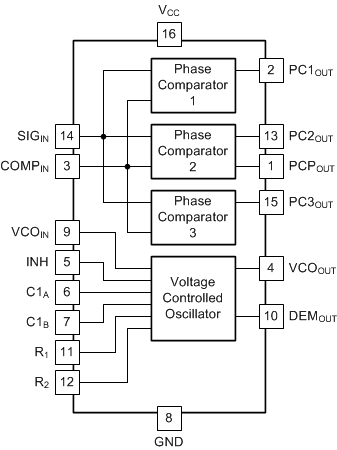
The SN74LV4046A is a high-speed silicon-gate CMOS device that is pin compatible with the
CD4046B and the CD74HC4046. The device is specified in compliance with JEDEC Std 7.The SN74LV4046A is a phase-locked loop (PLL) circuit that contains a linear
voltage-controlled oscillator (VCO) and three different phase comparators (PC1, PC2, and PC3). A
signal input and a comparator input are common to each comparator.The signal input can be directly coupled to large voltage signals, or indirectly coupled
(with a series capacitor) to small voltage signals. A self-bias input circuit keeps small voltage
signals within the linear region of the input amplifiers. With a passive low-pass filter, the
SN74LV4046A forms a second-order loop PLL. The excellent VCO linearity is achieved by the use of
linear operational amplifier techniques. Various applications include telecommunications, digital
phase-locked loop and signal generators.
SN74LV4046ANS 数据手册
SN74LV4046ANS 电路图