SN74LS73AN 供应商
-
SN74LS73AN
品牌:TI 封装/批号:原厂原装/22+ -
SN74LS73AN
品牌:TI(德州仪器) 封装/批号:PDIP-14/2022+ -
SN74LS73AN
品牌:TI 封装/批号:标准封装/23+ -
SN74LS73AN
品牌:M 封装/批号:PDIP/92+ -
SN74LS73AN
品牌:TI 封装/批号:/2021+ -
SN74LS73AN
品牌:TI 封装/批号:TSSOP/23+
SN74LS73AN 属性参数
- 标准包装:25
- 类别:集成电路 (IC)
- 家庭:逻辑 - 触发器
- 系列:74LS
- 功能:主复位
- 类型:JK 型
- 输出类型:差分
- 元件数:2
- 每个元件的位元数:1
- 频率 - 时钟:45MHz
- 延迟时间 - 传输:15ns
- 触发器类型:负边沿
- 输出电流高,低:400µA, 8mA
- 电源电压:4.75 V ~ 5.25 V
- 工作温度:0°C ~ 70°C
- 安装类型:通孔
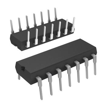
- 封装/外壳:14-DIP(0.300",7.62mm)
- 包装:管件
- 其它名称:296-26520-5SN74LS73AN-ND
产品特性
- Package Options Include Plastic “Small Outline" Packages, Flat Packages, and Plastic and Ceramic DIPs
- Dependable Texas Instruments Quality and Reliability
产品概述
The '73, and 'H73, contain two independent J-K flip-flops with individual
J-K, clock, and direct clear inputs. The '73, and 'H73, are positive pulse-triggered
flip-flops. J-K input is loaded into the master while the clock is high and
transferred to the slave on the high-to-low transition. For these devices
the J and K inputs must be stable while the clock is high.
The 'LS73A contains two independent negative-edge-triggered flip-flops.
The J and K inputs must be stable one setup time prior to the high-to-low
clock transition for predictable operation. When the clear is low, it overrides
the clock and data inputs forcing the Q output low and the Q\ output
high.
The SN5473, SN54H73, and the SN54LS73A are characterized for operation
over the full military temperature range of -55°C to 125°C. The SN7473,
and the SN74LS73A are characterized for operation from 0°C to 70°C.