SN74LS673DW 供应商
-
SN74LS673DW
品牌:TI 封装/批号:原厂原装/22+ -
SN74LS673DW
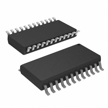
品牌:TI(德州仪器) 封装/批号:SOIC-24/2022+
SN74LS673DW 属性参数
- 标准包装:25
- 类别:集成电路 (IC)
- 家庭:逻辑 - 移位寄存器
- 系列:74LS
- 逻辑类型:移位寄存器
- 输出类型:标准
- 元件数:1
- 每个元件的位元数:16
- 功能:串行至并行
- 电源电压:4.75 V ~ 5.25 V
- 工作温度:0°C ~ 70°C
- 安装类型:表面贴装
- 封装/外壳:24-SOIC(0.295",7.50mm 宽)
- 供应商设备封装:24-SOIC
- 包装:管件
- 其它名称:296-3736-5
产品特性
- 'LS673 16-Bit Serial-In, Serial-Out Shift Register with 16-Bit Parallel-Out Storage Register Performs Serial-to-Parallel Conversion
- 16-Bit Serial-In, Serial-Out Shift Register with 16-Bit Parallel-Out Storage Register
- Performs Serial-to-Parallel Conversion
- 'LS674 16-Bit Parallel-In, Serial-Out Shift Register Performs Parallel-to-Serial Conversion
- 16-Bit Parallel-In, Serial-Out Shift Register
- Performs Parallel-to-Serial Conversion
产品概述
SN54LS673, SN74LS673
The 'LS673 is a 16-bit shift register and a 16-bit storage register in a single 24-pin package. A three-state input/output (SER/Q15) port to the shift register allows serial entry and/or reading of data. The storage register is connected in a parallel data loop with the shift register and may be asynchronously cleared by taking the store-clear input low. The storage register may be parallel loaded with shift-register data to provide shift-register status via the parallel outputs. The shift register can be parallel loaded with the storage-register data upon commmand.
A high logic level at the chip-level (CS\) input disables both the shift-register clock and the storage register clock and places SER/Q15 in the high-impedance state. The store-clear function is not disabled by the chip select.
Caution must be exercised to prevent false clocking of either the shift register or the storage register via the chip-select input. The shift clock should be low during the low-to-high transition of chip select and the store clock should be low during the high-to-low transition of chip select.
SN54LS674, SN74LS674
The 'LS674 is a 16-bit parallel-in, serial-out shift register. A three-state input/output (SER/Q15) port provides access for entering a serial data or reading the shift-register word in a recirculating loop.
The device has four basic modes of operation:
Low-to-high-level changes at the chip select input should be made only when the clock input is low to prevent false clocking.