SN74HC164DRG4 供应商
-
SN74HC164DRG4
品牌:TI 封装/批号:原厂原装/22+ -
SN74HC164DRG4
品牌:TI(德州仪器) 封装/批号:SOIC-14/2022+
SN74HC164DRG4 属性参数
- 标准包装:2,500
- 类别:集成电路 (IC)
- 家庭:逻辑 - 移位寄存器
- 系列:74HC
- 逻辑类型:移位寄存器
- 输出类型:标准
- 元件数:1
- 每个元件的位元数:8
- 功能:串行至并行
- 电源电压:2 V ~ 6 V
- 工作温度:-40°C ~ 85°C
- 安装类型:表面贴装
- 封装/外壳:14-SOIC(0.154",3.90mm 宽)
- 供应商设备封装:14-SOIC
- 包装:带卷 (TR)
产品特性
- Wide Operating Voltage Range of 2 V to 6 V
- Outputs Can Drive Up to 10 LSTTL Loads
- Low Power Consumption, 80-µA Maximum ICC
- Typical tpd = 20 ns
- ±4-mA Output Drive at 5 V
- Low Input Current of 1-µA Maximum
- AND-Gated (Enable/Disable) Serial Inputs
- Fully Buffered Clock and Serial Inputs
- Direct Clear
- On Products Compliant to MIL-PRF-38535, All Parameters Are Tested Unless Otherwise Noted. On All Other Products, Production Processing Does Not Necessarily Include Testing of All Parameters.
产品概述
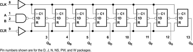
These 8-bit shift registers feature AND-gated serial inputs and an asynchronous clear
(CLR) input. The gated serial (A and B) inputs permit complete control over
incoming data; a low at either input inhibits entry of the new data and resets the first flip-flop
to the low level at the next clock (CLK) pulse. A high-level input enables the other input, which
then determines the state of the first flip-flop. Data at the serial inputs can be changed while
CLK is high or low, provided the minimum set-up time requirements are met. Clocking occurs on the
low-to-high-level transition of CLK.
SN74HC164DRG4 数据手册
SN74HC164DRG4 电路图