SN74GTL16622ADGGR 供应商
-
SN74GTL16622ADGGR
品牌:TI 封装/批号:原厂原装/22+
SN74GTL16622ADGGR 属性参数
- 标准包装:1
- 类别:集成电路 (IC)
- 家庭:逻辑 - 变换器
- 系列:74GTL
- 逻辑功能:变换器
- 位数:18
- 输入类型:LVTTL
- 输出类型:GTL
- 数据速率:-
- 通道数:2
- 输出/通道数目:9
- 差分 - 输入:输出:无/无
- 传输延迟(最大):5ns
- 电源电压:3.3V
- 工作温度:-40°C ~ 85°C
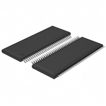
- 封装/外壳:64-TFSOP (0.240",6.10mm 宽)
- 供应商设备封装:64-TSSOP
- 包装:®
- 其它名称:296-1186-6
产品特性
- Member of Texas Instruments' Widebus™ Family
- D-Type Flip-Flops With Qualified Storage Enable
- Translates Between GTL/GTL+ Signal Levels and LVTTL Logic Levels
- Supports Mixed-Mode (3.3 V and 5 V) Signal Operation on A-Port and Control Inputs
- Ioff Supports Partial-Power-Down Mode Operation
- Bus Hold on Data Inputs Eliminates the Need for External Pullup/Pulldown Resistors on A Port
- Distributed VCC and GND Pins Minimize High-Speed Noise
- Latch-Up Performance Exceeds 250 mA Per JESD 17
- ESD Protection Exceeds JESD 22 2000-V Human-Body Model (A114-A) 200-V Machine Model (A115-A) 1000-V Charged-Device Model (C101)
- 2000-V Human-Body Model (A114-A)
- 200-V Machine Model (A115-A)
- 1000-V Charged-Device Model (C101)
产品概述
The SN74GTL16622A is an 18-bit registered bus transceiver that provides LVTTL-to-GTL/GTL+
and GTL/GTL+-to-LVTTL signal-level translation. This device is partitioned as two separate 9-bit
transceivers with individual clock-enable controls and contains D-type flip-flops for temporary
storage of data flowing in either direction. This device provides an interface between cards
operating at LVTTL logic levels and a backplane operating at GTL/GTL+ signal levels. Higher
speed operation is a direct result of the reduced output swing (<1 V), reduced input threshold
levels, and OEC™ circuitry.
The user has the flexibility of using this device at either GTL (VTT = 1.2 V and VREF = 0.8 V) or the preferred
higher noise margin GTL+ (VTT = 1.5 V and VREF = 1 V) signal levels. GTL+ is the Texas Instruments derivative
of the Gunning Transceiver Logic (GTL) JEDEC standard JESD 8-3. The B port normally operates at GTL or
GTL+ signal levels, while the A-port and control inputs are compatible with LVTTL logic levels and are 5-V
tolerant. VREF is the reference input voltage for the B port.
Data flow in each direction is controlled by the output-enable (OEAB\ and OEBA\) and clock (CLKAB and CLKBA)
inputs. The clock-enable (CEAB\ and CEBA\) inputs control each 9-bit transceiver independently, which makes
the device more versatile.
For A-to-B data flow, the device operates on the low-to-high transition of CLKAB if CEAB\ is low. When OEAB\
is low, the outputs are active. When OEAB\ is high, the outputs are in the high-impedance state. Data flow for
B to A is similar to that of A to B, but uses OEBA\, CLKBA, and CEBA\.
This device is fully specified for partial-power-down applications using Ioff. The Ioff circuitry disables the outputs,
preventing damaging current backflow through the device when it is powered down.
Active bus-hold circuitry holds unused or undriven LVTTL inputs at a valid logic state. Use of pullup or pulldown
resistors with the bus-hold circuitry is not recommended.
To ensure the high-impedance state during power up or power down, OE\ should be tied to VCC through a pullup
resistor; the minimum value of the resistor is determined by the current-sinking capability of the driver.