SN74F377AN 供应商
-
SN74F377AN
品牌:TI 封装/批号:原厂原装/22+ -
SN74F377AN
品牌:TI 封装/批号:/2019+ -
SN74F377AN
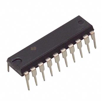
品牌:TI(德州仪器) 封装/批号:PDIP-20/2022+ -
SN74F377AN
品牌:TI 封装/批号:DIP-20/23+
SN74F377AN 属性参数
- 标准包装:20
- 类别:集成电路 (IC)
- 家庭:逻辑 - 触发器
- 系列:74F
- 功能:标准
- 类型:D 型总线
- 输出类型:三态非反相
- 元件数:1
- 每个元件的位元数:8
- 频率 - 时钟:125MHz
- 延迟时间 - 传输:6.5ns
- 触发器类型:正边沿
- 输出电流高,低:1mA,20mA
- 电源电压:4.5 V ~ 5.5 V
- 工作温度:0°C ~ 70°C
- 安装类型:通孔
- 封装/外壳:20-DIP(0.300",7.62mm)
- 包装:管件
- 其它名称:296-33911-5SN74F377AN-ND
产品特性
- Contains Eight D-Type Flip-Flops With Single-Rail Outputs
- Clock Enable Latched to Avoid False Clocking
- Applications Include:
- Buffer/Storage Registers
- Shift Registers
- Pattern Generators
- Buffered Common Enable Input
- Package Options Include Plastic Small-Outline Packages and Standard Plastic 300-mil DIPs
产品概述
The SN74F377A is a monolithic, positive-edge-triggered, octal,
D-type flip-flop with clock enable inputs. The SN74F377A features a
latched clock enable ()
input.Information at the data (D) inputs meeting the setup time
requirements is transferred to the Q outputs on the positive-going
edge of the clock pulse if is
low. Clock triggering occurs at a particular voltage level and is not
directly related to the positive-going pulse. When the clock input is
at either the high or low level, the D input signal has no effect at
the output. The circuits are designed to prevent false clocking by
transitions at the
input.The SN74F377A is characterized for operation from 0°C to
70°C.