SN74CB3Q3125DGVR 供应商
-
SN74CB3Q3125DGVR
品牌:TI 封装/批号:原厂原装/22+
SN74CB3Q3125DGVR 属性参数
- 标准包装:1
- 类别:集成电路 (IC)
- 家庭:逻辑 - 信号开关,多路复用器,解码器
- 系列:74CB
- 类型:FET 总线开关
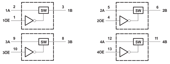
- 电路:1 x 1:1
- 独立电路:4
- 输出电流高,低:15mA,30mA
- 电压电源:单电源
- 电源电压:2.3 V ~ 3.6 V
- 工作温度:-40°C ~ 85°C
- 安装类型:表面贴装
- 封装/外壳:14-TFSOP (0.173",4.40mm 宽)
- 供应商设备封装:14-TVSOP
- 包装:®
- 其它名称:296-19124-6
产品特性
- High-Bandwidth Data Path (up to 500 MHz(1))
- 5-V Tolerant I/Os With Device Powered Up or Powered Down
- Low and Flat ON-State Resistance (ron) Characteristics Over Operating Range (ron = 3 Ω Typ)
- Rail-to-Rail Switching on Data I/O Ports 0-V to 5-V Switching With 3.3-V VCC 0-V to 3.3-V Switching With 2.5-V VCC
- 0-V to 5-V Switching With 3.3-V VCC
- 0-V to 3.3-V Switching With 2.5-V VCC
- Bidirectional Data Flow With Near-Zero Propagation Delay
- Low Input and Output Capacitance Minimizes Loading and Signal Distortion (Cio(OFF) = 4 pF Typ)
- Fast Switching Frequency (fOE = 20 MHz Max)
- Data and Control Inputs Provide Undershoot Clamp Diodes
- Low Power Consumption (ICC = 0.3 mA Typ)
- VCC Operating Range From 2.3 V to 3.6 V
- Data I/Os Support 0-V to 5-V Signaling Levels (0.8 V, 1.2 V, 1.5 V, 1.8 V, 2.5 V, 3.3 V, 5 V)
- Control Inputs Can Be Driven by TTL, 5-V, or 3.3-V CMOS Outputs
- Ioff Supports Partial-Power-Down Mode Operation
- Latch-Up Performance Exceeds 100 mA Per JESD 78, Class II
- ESD Performance Tested Per JESD 22 2000-V Human-Body Model (A114-B, Class II) 1000-V Charged-Device Model (C101)
- 2000-V Human-Body Model (A114-B, Class II)
- 1000-V Charged-Device Model (C101)
- Supports Both Digital and Analog Applications: USB Interface, Differential Signal Interface, Bus Isolation, Low-Distortion Signal Gating
产品概述
The SN74CB3Q3125 device is a high-bandwidth FET bus switch that uses a charge pump to
elevate the gate voltage of the pass transistor, thus providing a low and flat ON-state resistance
(ron). The low and flat ON-state resistance allows for minimal propagation
delay and supports rail-to-rail switching on the data input/output (I/O) ports. The SN74CB3Q3125
device also features low data I/O capacitance to minimize capacitive loading and signal distortion
on the data bus.
SN74CB3Q3125DGVR 数据手册
SN74CB3Q3125DGVR 电路图