SN74BCT29854DW 供应商
-
SN74BCT29854DW
品牌:TI 封装/批号:原厂原装/22+
SN74BCT29854DW 属性参数
- 标准包装:150
- 类别:集成电路 (IC)
- 家庭:逻辑 - 专用逻辑
- 系列:74BCT
- 逻辑类型:8 位至 9 位奇偶总线收发器
- 电源电压:4.5 V ~ 5.5 V
- 位数:8
- 工作温度:0°C ~ 70°C
- 安装类型:表面贴装
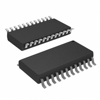
- 封装/外壳:24-SOIC(0.295",7.50mm 宽)
- 供应商设备封装:24-SOIC
- 包装:管件
产品特性
- BiCMOS Process With TTL Inputs and Outputs
- State-of-the-Art BiCMOS Design Significantly Reduces Standby Current
- Flow-Through Pinout (All Inputs on Opposite Side From Outputs)
- Functionally Equivalent to AMD Am29854
- High-Speed Bus Transceiver With Parity Generator/Checker
- Parity-Error Flag With Open-Collector Output
- Latch for Storage of the Parity-Error Flag
- Package Options Include Plastic Small-Outline (DW) Packages and Standard Plastic 300-mil DIPs (NT)
产品概述
The SN74BCT29854 is an 8-bit to 9-bit parity transceiver designed
for asynchronous communication between data buses. When data is
transmitted from the A to B bus, a parity bit is generated. When data
is transmitted from the B to A bus with its corresponding parity bit,
the parity-error () output will
indicate whether or not an error in the B data has occurred. The
output-enable (, ) inputs can be used to disable the
device so that the buses are effectively isolated.A 9-bit parity generator/checker generates a parity-odd (PARITY)
output and monitors the parity of the I/O ports with an
open-collector parity-error () flag. can
be either passed, sampled, stored, or cleared from the latch using
the latch-enable () and clear
() control
inputs. When both and are low, data is transferred from
the A bus to the B bus and inverted parity is generated. Inverted
parity is a forced error condition which gives the designer more
system diagnostic capability. The SN74BCT29854 provides inverting
logic.The SN74BCT29854 is characterized for operation from 0°C to
70°C.