SN74AUP1G06DSF2 供应商
-
SN74AUP1G06DSF2
品牌:TI 封装/批号:原厂原装/22+ -
SN74AUP1G06DSF2
品牌:TI(德州仪器) 封装/批号:SON-6/2022+
SN74AUP1G06DSF2 属性参数
- 现有数量:3,634现货10,000Factory
- 价格:1 : ¥4.77000剪切带(CT)5,000 : ¥1.89605卷带(TR)
- 系列:74AUP
- 包装:卷带(TR)剪切带(CT)? 得捷定制卷带
- 产品状态:在售
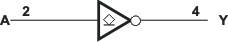
- 逻辑类型:反相器
- 电路数:1
- 输入数:1
- 特性:开路漏极
- 电压 - 供电:0.8V ~ 3.6V
- 电流 - 静态(最大值):500 nA
- 电流 - 输出高、低:-,4mA
- 逻辑电平 - 低:0.1V ~ 0.45V
- 逻辑电平 - 高:3.6V
- 不同 V、最大 CL 时最大传播延迟:10.5ns @ 3.3V,30pF
- 工作温度:-40°C ~ 85°C(TA)
- 安装类型:表面贴装型
- 供应商器件封装:6-SON(1x1)
- 封装/外壳:6-XFDFN
产品特性
- Latch-Up Performance Exceeds 100 mA Per JESD 78, Class II
- ESD Performance Tested Per JESD 222000-V Human-Body Model (A114-B, Class II)1000-V Charged-Device Model (C101)
- 2000-V Human-Body Model (A114-B, Class II)
- 1000-V Charged-Device Model (C101)
- Available in the Texas Instruments NanoStar™ Package
- Low Static-Power Consumption (ICC = 0.9 µA Maximum)
- Low Dynamic-Power Consumption (Cpd = 1 pF Typical at 3.3 V)
- Low Input Capacitance (Ci = 1.5 pF Typical)
- Low Noise – Overshoot and Undershoot <10% of VCC
- Ioff Supports Partial Power-Down-Mode Operation
- Input Hysteresis Allows Slow Input Transition and Better Switching Noise Immunity at the Input (Vhys = 250 mV Typical at 3.3 V)
- Wide Operating VCC Range of 0.8 V to 3.6 V
- Optimized for 3.3-V Operation
- 3.6-V I/O Tolerant to Support Mixed-Mode Signal Operation
- tpd = 3.6 ns Maximum at 3.3 V
- Suitable for Point-to-Point Applications
产品概述
The AUP family is TI’s premier solution to the industry’s low-power needs in
battery-powered portable applications. This family ensures a very low static and dynamic power
consumption across the entire VCC range of 0.8 V to 3.6 V, resulting in an
increased battery life. This product also maintains excellent signal integrity (see
AUP – The Lowest-Power Family and Excellent Signal Integrity).
SN74AUP1G06DSF2 电路图