SN74AUP1G00DRLR 供应商
-
SN74AUP1G00DRLR 原装现货
品牌:TI 封装/批号:SOT553/17+ -
SN74AUP1G00DRLR
品牌:TI 封装/批号:原厂原装/22+
SN74AUP1G00DRLR 属性参数
- 标准包装:1
- 类别:集成电路 (IC)
- 家庭:逻辑 - 栅极和逆变器
- 系列:74AUP
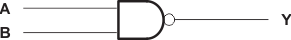
- 逻辑类型:与非门
- 电路数:1
- 输入数:2
- 特点:-
- 电源电压:0.8 V ~ 3.6 V
- 电流 - 静态(最大值):0.5µA
- 输出电流高,低:4mA,4mA
- 逻辑电平 - 低:0.7 V ~ 0.9 V
- 逻辑电平 - 高:1.6 V ~ 2 V
- 额定电压和最大 CL 时的最大传播延迟:6.5ns @ 3V ~ 3.6V,30pF
- 工作温度:-40°C ~ 85°C
- 安装类型:表面贴装
- 供应商设备封装:SOT-5
- 封装/外壳:SOT-553
- 包装:®
- 其它名称:296-18712-6
产品特性
- ESD Performance Tested Per JESD 22 2000-V Human-Body Model (A114-B, Class II) 1000-V Charged-Device Model (C101)
- 2000-V Human-Body Model (A114-B, Class II)
- 1000-V Charged-Device Model (C101)
- Available in the Ultra Small 0.64 mm2 Package (DPW) with 0.5-mm Pitch
- Low Static-Power Consumption (ICC = 0.9 µA Max)
- Low Dynamic-Power Consumption (Cpd = 4 pF Typical at 3.3 V)
- Low Input Capacitance (Ci = 1.5 pF Typical)
- Low Noise Overshoot and Undershoot <10% of VCC
- Ioff Supports Live Insertion, Partial-Power-Down Mode, and Back-Drive Protection
- Input Hysteresis Allows Slow Input Transition and Better Switching Noise Immunity at Input (Vhys = 250 mV Typical at 3.3 V)
- Wide Operating VCC Range of 0.8 V to 3.6 V
- Optimized for 3.3-V Operation
- 3.6-V I/O Tolerant to Support Mixed-Mode Signal Operation
- tpd = 4.8 ns Maximum at 3.3 V
- Suitable for Point-to-Point Applications
- Latch-Up Performance Exceeds 100 mA Per JESD 78, Class II
产品概述
This single 2-input positive-NAND gate performs the Boolean function Y = A ×
B or Y = A + B in positive logic.
SN74AUP1G00DRLR 数据手册
SN74AUP1G00DRLR 电路图