SN74AS832BN 供应商
-
SN74AS832BN
品牌:TI 封装/批号:原厂原装/22+
SN74AS832BN 属性参数
- 标准包装:20
- 类别:集成电路 (IC)
- 家庭:逻辑 - 栅极和逆变器
- 系列:74AS
- 逻辑类型:或门
- 电路数:6
- 输入数:2
- 特点:-
- 电源电压:4.5 V ~ 5.5 V
- 电流 - 静态(最大值):-
- 输出电流高,低:48mA,48mA
- 逻辑电平 - 低:0.8V
- 逻辑电平 - 高:2V
- 额定电压和最大 CL 时的最大传播延迟:6.3ns @ 4.5V ~ 5.5V,50pF
- 工作温度:0°C ~ 70°C
- 安装类型:通孔
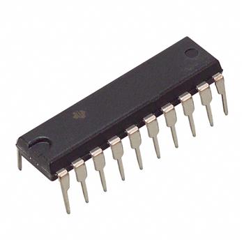
- 供应商设备封装:20-PDIP
- 封装/外壳:20-DIP(0.300",7.62mm)
- 包装:管件
- 其它名称:296-33821-5SN74AS832BN-ND
产品特性
- High Capacitive-Drive Capability
- ´ALS832A Has Typical Delay Time of 4.8 ns (CL = 50 pF) and Typical Power Dissipation of 4.5 mW Per Gate
- ´AS832B Has Typical Delay Time of 3.2 ns (CL = 50 pF) and Typical Power Dissipation of Less Than 13 mW Per Gate
- Package Options Include Plastic Small-Outline (DW) Packages, Ceramic Chip Carriers (FK), and Standard Plastic (N) and Ceramic (J) 300-mil DIPs
产品概述
These devices contain six independent 2-input OR drivers. They
perform the Boolean functions Y = A + B orin positive logic. The SN54ALS832A and SN54AS832B are characterized for operation
over the full military temperature range of -55°C to 125°C.
The SN74ALS832A and SN74AS832B are characterized for operation from
0°C to 70°C.