SN74ALVCH16524DL 供应商
-
SN74ALVCH16524DL
品牌:TI 封装/批号:原厂原装/22+ -
SN74ALVCH16524DL
品牌:TI 封装/批号:/2019+ -
SN74ALVCH16524DL
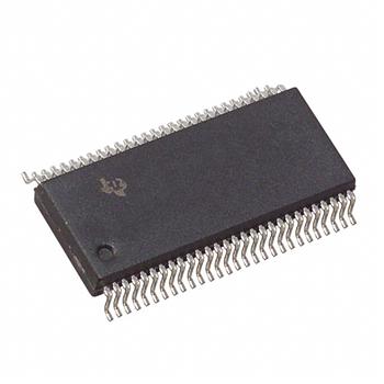
品牌:TI(德州仪器) 封装/批号:SSOP-56/2022+
SN74ALVCH16524DL 属性参数
- 标准包装:20
- 类别:集成电路 (IC)
- 家庭:逻辑 - 通用总线函数
- 系列:74ALVCH
- 逻辑类型:通用总线收发器
- 输入数:-
- 电路数:18 位
- 输出电流高,低:24mA,24mA
- 电源电压:1.65 V ~ 3.6 V
- 工作温度:-40°C ~ 85°C
- 安装类型:表面贴装
- 封装/外壳:56-BSSOP(0.295",7.50mm 宽)
- 供应商设备封装:56-SSOP
- 包装:管件
- 其它名称:296-12870-5
产品特性
- Member of the Texas Instruments Widebus™ Family
- UBT™ Transceiver Combines D-Type Latches and D-Type Flip-Flops for Operation in Transparent, Latched, Clocked, or Clock-Enable Mode
- Operates From 1.65-V to 3.6-V
- Max tpd of 3.2 ns at 3.3-V
- ±24-mA Output Drive at 3.3-V
- Bus Hold on Data Inputs Eliminates the Need for External Pullup/Pulldown Resistors
- Latch-Up Performance Exceeds 250 mA Per JESD 17
- ESD Performance Tested Per JESD 22 2000-V Human-Body Model (A114-A) 200-V Machine Model (A115-A)
- 2000-V Human-Body Model (A114-A)
- 200-V Machine Model (A115-A)
产品概述
This 18-bit universal bus transceiver is designed for 1.65-V to 3.6-V VCC operation.Data flow in each direction is controlled by output-enable (OEAB\ and OEBA\) and clock-enable (CLKENBA\) inputs. For the A-to-B data flow, the data flows through a single buffer. The B-to-A data can flow through a four-stage pipeline register path, or through a single register path, depending on the state of the select (SEL\) input.Data is stored in the internal registers on the low-to-high transition of the clock (CLK) input, provided that the appropriate CLKENBA\ input is low. The B-to-A data transfer is synchronized with CLK.To ensure the high-impedance state during power up or power down, OE\ should be tied to VCC through a pullup resistor; the minimum value of the resistor is determined by the current-sinking capability of the driver.Active bus-hold circuitry holds unused or undriven inputs at a valid logic state. Use of pullup or pulldown resistors with the bus-hold circuitry is not recommended.