SN74ALVCH16270DL 供应商
-
SN74ALVCH16270DL
品牌:TI 封装/批号:原厂原装/22+ -
SN74ALVCH16270DL
品牌:TI 封装/批号:SSOP56/2019+
SN74ALVCH16270DL 属性参数
- 标准包装:20
- 类别:集成电路 (IC)
- 家庭:逻辑 - 通用总线函数
- 系列:74ALVCH
- 逻辑类型:寄存总线交换器
- 输入数:-
- 电路数:12 至 24 位
- 输出电流高,低:24mA,24mA
- 电源电压:1.65 V ~ 3.6 V
- 工作温度:-40°C ~ 85°C
- 安装类型:表面贴装
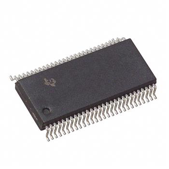
- 封装/外壳:56-BSSOP(0.295",7.50mm 宽)
- 供应商设备封装:56-SSOP
- 包装:管件
- 其它名称:296-5201-5
产品特性
- Member of the Texas Instruments Widebus™ Family
- EPIC™ (Enhanced-Performance Implanted CMOS) Submicron Process
- Bus Hold on Data Inputs Eliminates the Need for External Pullup/Pulldown Resistors
- ESD Protection Exceeds 2000 V Per MIL-STD-883, Method 3015; Exceeds 200 V Using Machine Model (C = 200 pF, R = 0)
- Latch-Up Performance Exceeds 250 mA Per JESD 17
- Package Options Include Plastic Shrink Small-Outline (DL) and Thin Shrink Small-Outline (DGG) Packages
产品概述
This 12-bit to 24-bit registered bus exchanger is designed for 1.65-V to 3.6-V VCC operation.The SN74ALVCH16270 is used in applications in which data must be transferred from a narrow high-speed bus to a wide lower-frequency bus.The device provides synchronous data exchange between the two ports. Data is stored in the internal registers on the low-to-high transition of the clock (CLK) input when the appropriate CLKEN\ inputs are low. The select (SEL)\ line selects 1B or 2B data for the A outputs. For data transfer in the A-to-B direction, a two-stage pipeline is provided in the A-to-1B path, with a single storage register in the A-to-2B path. Proper control of the CLKENA\ inputs allows two sequential 12-bit words to be presented synchronously as a 24-bit word on the B port. Data flow is controlled by the active-low output enables (OEA\, OEB\). The control terminals are registered to synchronize the bus-direction changes with CLK.To ensure the high-impedance state during power up or power down, a clock pulse should be applied as soon as possible, and OE\ should be tied to VCC through a pullup resistor; the minimum value of the resistor is determined by the current-sinking capability of the driver. Due to OE\ being routed through a register, the active state of the outputs cannot be determined prior to the arrival of the first clock pulse.Active bus-hold circuitry is provided to hold unused or floating data inputs at a valid logic level.The SN74ALVCH16270 is characterized for operation from –40°C to 85°C.