SN74ALVC162334DGGR 供应商
-
SN74ALVC162334DGGR
品牌:TI 封装/批号:原厂原装/22+ -
SN74ALVC162334DGGR
品牌:TI 封装/批号:可控硅/23+
SN74ALVC162334DGGR 属性参数
- 标准包装:1
- 类别:集成电路 (IC)
- 家庭:逻辑 - 通用总线函数
- 系列:74ALVC
- 逻辑类型:通用总线驱动器
- 输入数:-
- 电路数:16 位
- 输出电流高,低:12mA,12mA
- 电源电压:1.65 V ~ 3.6 V
- 工作温度:-40°C ~ 85°C
- 安装类型:表面贴装
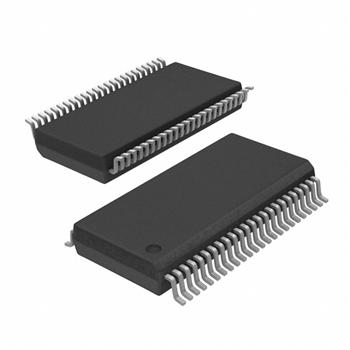
- 封装/外壳:48-TFSOP(0.240",6.10mm 宽)
- 供应商设备封装:48-TSSOP
- 包装:®
- 其它名称:296-1131-6
产品特性
- Member of the Texas Instruments Widebus™ Family
- Ideal for Use in PC100 Register DIMM
- Operates From 1.65 V to 3.6 V
- Max tpd of 3.8 ns at 3.3 V
- ±12-mA Output Drive at 3.3 V
- Output Ports Have Equivalent 26- Series Resistors, So No External Resistors Are Required
- Designed to Comply With JEDEC 168-Pin and 200-Pin SDRAM Buffered DIMM Specification
- Latch-Up Performance Exceeds 250 mA Per JESD 17
- ESD Protection Exceeds JESD 22 2000-V Human-Body Model (A114-A) 200-V Machine Model (A115-A) 1000-V Charged-Device Model (C101)
- 2000-V Human-Body Model (A114-A)
- 200-V Machine Model (A115-A)
- 1000-V Charged-Device Model (C101)
产品概述
This 16-bit universal bus driver is designed for 1.65-V to 3.6-V VCC operation.Data flow from A to Y is controlled by the output-enable (OE\) input. The device operates in the transparent mode when the latch-enable (LE\) input is low. When LE\ is high, the A data is latched if the clock (CLK) input is held at a high or low logic level. If LE\ is high, the A data is stored in the latch/flip-flop on the low-to-high transition of CLK. When OE\ is high, the outputs are in the high-impedance state.The outputs, which are designed to sink up to 12 mA, include equivalent 26- resistors to reduce overshoot and undershoot.To ensure the high-impedance state during power up or power down, OE\ should be tied to VCC through a pullup resistor; the minimum value of the resistor is determined by the current-sinking capability of the driver.