SN74ALS29821DW 供应商
-
SN74ALS29821DW
品牌:TI 封装/批号:原厂原装/22+
SN74ALS29821DW 属性参数
- 标准包装:25
- 类别:集成电路 (IC)
- 家庭:逻辑 - 触发器
- 系列:74ALS
- 功能:标准
- 类型:D 型总线
- 输出类型:非反相
- 元件数:1
- 每个元件的位元数:10
- 频率 - 时钟:-
- 延迟时间 - 传输:2ns
- 触发器类型:正边沿
- 输出电流高,低:24mA,48mA
- 电源电压:4.75 V ~ 5.25 V
- 工作温度:0°C ~ 70°C
- 安装类型:表面贴装
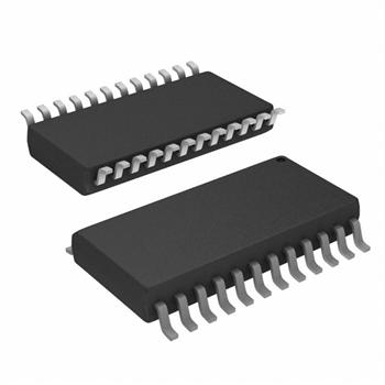
- 封装/外壳:24-SOIC(0.295",7.50mm 宽)
- 包装:管件
产品特性
- Functionally Equivalent to AMD's AM29821
- Provide Extra Data Width Necessary for Wider Address/Data Paths or Buses With Parity
- Outputs Have Undershoot-Protection Circuitry
- Power-Up High-Impedance State
- Buffered Control Inputs Reduce dc Loading Effects
- Package Options Include Plastic Small-Outline (DW) Packages and Standard Plastic (NT) and Ceramic (JT) 300-mil DIPs
产品概述
These 10-bit edge-triggered D-type flip-flops feature 3-state
outputs designed specifically for driving highly capacitive or
relatively low-impedance loads. These devices are particularly
suitable for implementing wider buffer registers, I/O ports,
bidirectional bus drivers with parity, and working registers.On the positive transition of the clock (CLK) input, the Q outputs
are true to the data (D) input.A buffered output-enable () input can place the ten outputs in either a normal
logic state (high or low logic levels) or a high-impedance state. The
outputs also are in the high-impedance state during power-up and
power-down conditions. The outputs remain in the high-impedance state
while the device is powered down. In the high-impedance state, the
outputs neither load nor drive the bus lines significantly. The
high-impedance state and increased drive provide the capability to
drive bus lines without interface or pullup components.does not affect
the internal operation of the flip-flops. Old data can be retained or
new data can be entered while the outputs are in the high-impedance
state.The SN54ALS29821 is characterized for operation over the full
military temperature range of -55°C to 125°C. The
SN74ALS29821 is characterized for operation from 0°C to
70°C.