SN74AHC273NSR 供应商
-
SN74AHC273NSR
品牌:TI 封装/批号:原厂原装/22+
SN74AHC273NSR 属性参数
- 标准包装:1
- 类别:集成电路 (IC)
- 家庭:逻辑 - 触发器
- 系列:74AHC
- 功能:主复位
- 类型:D 型总线
- 输出类型:非反相
- 元件数:1
- 每个元件的位元数:8
- 频率 - 时钟:110MHz
- 延迟时间 - 传输:1ns
- 触发器类型:正边沿
- 输出电流高,低:8mA,8mA
- 电源电压:2 V ~ 5.5 V
- 工作温度:-40°C ~ 85°C
- 安装类型:表面贴装
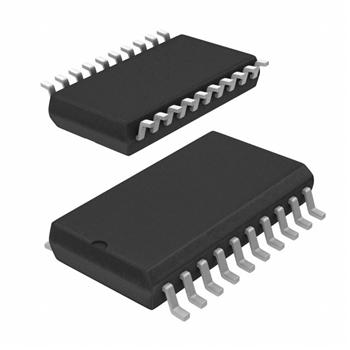
- 封装/外壳:20-SOIC(0.209",5.30mm 宽)
- 包装:®
- 其它名称:296-29969-6
产品特性
- Operating Range 2-V to 5.5-V VCC
- Contain Eight Flip-Flops With Single-Rail Outputs
- Direct Clear Input
- Individual Data Input to Each Flip-Flop
- Latch-Up Performance Exceeds 250 mA Per JESD 17
- ESD Protection Exceeds JESD 22 2000-V Human-Body Model (A114-A) 1000-V Charged-Device Model (C101)
- 2000-V Human-Body Model (A114-A)
- 1000-V Charged-Device Model (C101)
- On Products Compliant to MIL-PRF-38535, All Parameters Are Tested Unless Otherwise Noted. On All Other Products, Production Processing Does Not Necessarily Include Testing of All Parameters.
产品概述
These devices are positive-edge-triggered D-type
flip-flops with a direct clear (CLR) input.Information at the data (D) inputs meeting the setup time requirements is transferred to
the Q outputs on the positive-going edge of the clock (CLK) pulse. Clock triggering occurs at a
particular voltage level and is not directly related to the transition time of the positive-going
pulse. When CLK is at either the high or low level, the D input has no effect at the output.