SN74ABT16823DL 供应商
-
SN74ABT16823DL
品牌:TI 封装/批号:原厂原装/22+ -
SN74ABT16823DLR
品牌:TI(德州仪器) 封装/批号:SSOP-56/2022+
SN74ABT16823DL 属性参数
- 标准包装:20
- 类别:集成电路 (IC)
- 家庭:逻辑 - 触发器
- 系列:74ABT
- 功能:主复位
- 类型:D 型总线
- 输出类型:三态非反相
- 元件数:2
- 每个元件的位元数:9
- 频率 - 时钟:150MHz
- 延迟时间 - 传输:3.9ns
- 触发器类型:正边沿
- 输出电流高,低:32mA,64mA
- 电源电压:4.5 V ~ 5.5 V
- 工作温度:-40°C ~ 85°C
- 安装类型:表面贴装
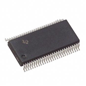
- 封装/外壳:56-BSSOP(0.295",7.50mm 宽)
- 包装:管件
- 其它名称:296-33617-5SN74ABT16823DL-ND
产品特性
- Members of the Texas Instruments WidebusTM Family
- State-of-the-Art EPIC-IIBTM BiCMOS Design Significantly Reduces Power Dissipation
- High-Impedance State During Power Up and Power Down
- ESD Protection Exceeds 2000 V Per MIL-STD-883, Method 3015; Exceeds 200 V Using Machine Model (C = 200 pF, R = 0)
- Typical VOLP (Output Ground Bounce) < 1 V at VCC = 5 V, TA = 25°C
- Distributed VCC and GND Pin Configuration Minimizes High-Speed Switching Noise
- Flow-Through Architecture Optimizes PCB Layout
- High-Drive Outputs (-32-mA IOH, 64-mA IOL)
- Package Options Include Plastic 300-mil Shrink Small-Outline (DL), Thin Shrink Small-Outline (DGG) Packages and 380-mil Fine-Pitch Ceramic Flat (WD) Package Using 25-mil Center-to-Center Spacings
产品概述
These 18-bit flip-flops feature 3-state outputs designed
specifically for driving highly capacitive or relatively
low-impedance loads. They are particularly suitable for implementing
wider buffer registers, I/O ports, bidirectional bus drivers with
parity, and working registers.The 'ABT16823 can be used as two 9-bit flip-flops or one 18-bit
flip-flop. With the clock-enable () input low, the D-type flip-flops enter data on the
low-to-high transitions of the clock. Taking high disables the clock buffer,
latching the outputs. Taking the clear () input low causes the Q outputs to
go low independently of the clock.A buffered output-enable () input can be used to place the nine outputs in either
a normal logic state (high or low logic level) or a high-impedance
state. In the high-impedance state, the outputs neither load nor
drive the bus lines significantly. The high-impedance state and
increased drive provide the capability to drive bus lines without
need for interface or pullup components.does not affect
the internal operation of the flip-flops. Old data can be retained or
new data can be entered while the outputs are in the high-impedance
state. When VCC is between 0 and 2.1 V, the device is in the
high-impedance state during power up or power down. However, to
ensure the high-impedance state above 2.1 V, should be tied to VCC
through a pullup resistor; the minimum value of the resistor is
determined by the current-sinking/current-sourcing capability of the
driver.The SN54ABT16823 is characterized for operation over the full
military temperature range of -55°C to 125°C. The
SN74ABT16823 is characterized for operation from -40°C to
85°C.