SN65LVCP202RGER 供应商
-
SN65LVCP202RGER
品牌:TI 封装/批号:原厂原装/22+ -
SN65LVCP202RGER
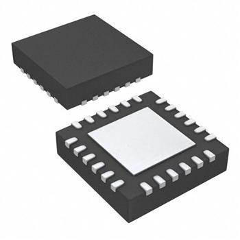
品牌:TI(德州仪器) 封装/批号:VQFN-24(4x4)/2022+
SN65LVCP202RGER 属性参数
- 标准包装:1
- 类别:集成电路 (IC)
- 家庭:接口 - 模拟开关,多路复用器,多路分解器
- 系列:65LVCP
- 功能:交叉点开关
- 电路:1 x 2:2
- 导通状态电阻:-
- 电压电源:单电源
- 电压 - 电源,单路/双路(±):3.14 V ~ 3.47 V
- 电流 - 电源:115mA
- 工作温度:-40°C ~ 85°C
- 安装类型:表面贴装
- 封装/外壳:24-VFQFN 裸露焊盘
- 供应商设备封装:24-VQFN 裸露焊盘(4x4)
- 包装:®
- 其它名称:296-24338-6
产品特性
- Up to 2.5-Gbps Operation
- Nonblocking Architecture Allows Each Output to Be Connected to Any Input
- 30 ps of Deterministic Jitter
- Selectable Transmit Preemphasis Per Lane
- Receive Equalization
- Available Packaging: 24-Pin QFN
- Propagation Delay Times: 500 ps Typical
- Inputs Electrically Compatible With CML Signal Levels
- Operates From a Single 3.3-V Supply
- Outputs Can Be Driven to Hi-Z State
- Low Power: 290 mW (typ)
- Integrated Termination Resistors
- APPLICATIONS Clock Buffering/Clock MUXing Wireless Base Stations High-Speed Network Routing Telecom/Datacom
- Clock Buffering/Clock MUXing
- Wireless Base Stations
- High-Speed Network Routing
- Telecom/Datacom
产品概述
The SN65LVCP202 is a 2 × 2 nonblocking crosspoint switch in a flow-through pinout allowing for ease in PCB layout. VML signaling is used to achieve a high-speed data throughput while using low power. Each of the output drivers includes a 2:1
multiplexer to allow any input to be routed to any output. Internal signal paths are fully differential to achieve high signaling speeds while maintaining low signal skews. The SN65LVCP202 incorporates 100-
termination resistors for those applications where board space is at a premium. Transmit preemphasis and receive equalization are built in for superior signal integrity performance.The SN65LVCP202 is characterized for operation from –40°C to 85°C.