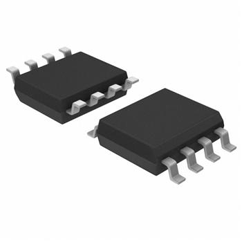
SN65LBC176AQDREP 供应商
-
SN65LBC176AQDREP
品牌:TI 封装/批号:原厂原装/22+ -
SN65LBC176AQDREP
品牌:TI(德州仪器) 封装/批号:SOIC-8/2022+
SN65LBC176AQDREP 属性参数
- 标准包装:1
- 类别:集成电路 (IC)
- 家庭:接口 - 驱动器,接收器,收发器
- 系列:-
- 类型:收发器
- 驱动器/接收器数:1/1
- 规程:RS485
- 电源电压:4.75 V ~ 5.25 V
- 安装类型:表面贴装
- 封装/外壳:8-SOIC(0.154",3.90mm 宽)
- 供应商设备封装:8-SOIC
- 包装:®
- 其它名称:296-22241-6
产品特性
- Controlled Baseline One Assembly/Test Site, One Fabrication Site
- One Assembly/Test Site, One Fabrication Site
- Extended Temperature Performance of –40°C to 125°C
- Enhanced Diminishing Manufacturing Sources (DMS) Support
- Enhanced Product Change Notification
- Qualification Pedigree
- High-Speed Low-Power LinBiCMOS™ Circuitry Designed for Signaling Rates Up to 30 Mbps
- Bus-Pin ESD Protection Exceeds 12-kV HBM
- Compatible With ANSI Standard TIA/EIA-485-A and ISO 8482:1987(E)
- Low Skew
- Designed for Multipoint Transmission on Long Bus Lines in Noisy Environments
- Low Disabled Supply Current Requirements . . . 700 µA Maximum
- Common Mode Voltage Range of –7 V to 12 V
- Thermal-Shutdown Protection
- Driver Positive and Negative Current Limiting
- Open-Circuit Fail-Safe Receiver Design
- Receiver Input Sensitivity ...±200 mV Max
- Receiver Input Hysteresis . . . 50 mV Typ
- Glitch-Free Power-Up and Power-Down Protection
产品概述
The SN65LBC176A-EP differential bus transceiver is a monolithic, integrated circuits designed for bidirectional data communication on multipoint bus-transmission lines. The SN65LBC176A-EP is designed for balanced transmission lines and is compatible with ANSI standard TIA/EIA-485-A and ISO 8482. The SN65LBC176A-EP offers improved switching performance over its predecessors without sacrificing significantly more power.The SN65LBC176A-EP combines a 3-state, differential line driver and a differential input line receiver, both of which operate from a single 5-V power supply. The driver and receiver have active-high and active-low enables, respectively, which can externally connect together to function as a direction control. The driver differential outputs and the receiver differential inputs connect internally to form a differential input/output (I/O) bus port that is designed to offer minimum loading to the bus whenever the driver is disabled or VCC = 0. This port features wide positive and negative common-mode voltage ranges, making the device suitable for party-line applications. Low device supply current can be achieved by disabling the driver and the receiver.
